Check patentability & draft patents in minutes with Patsnap Eureka AI!

Organic electroluminescence device

a technology of electroluminescence and organic materials, which is applied in the direction of discharge tube luminescnet screens, natural mineral layered products, transportation and packaging, etc., can solve the problems of difficult to find optimal thickness values that optimize color coordinates and brightness for blue light, and achieve the effect of increasing the color purity and brightness of the color blu

Inactive Publication Date: 2005-09-15
SAMSUNG DISPLAY CO LTD
View PDF5 Cites 0 Cited by
  • Summary
  • Abstract
  • Description
  • Claims
  • Application Information

AI Technical Summary

Benefits of technology

This configuration significantly improves the color purity and brightness of blue light by carefully considering the light emitting characteristics and refractive index components across different wavelength bands, leading to enhanced optical performance.

Problems solved by technology

Although U.S. Pat. No. 6,124,024 suggests ranges for the total optical thickness of thin films that allow light to constructively interfere at each wavelength, the ranges of the total optical thickness of thin films are not optimized for both color coordinates and brightness.
However, the conditions of the sum of thicknesses of the organic layer, the transparent electrode, and the high-refraction layer determined by the formulas suggested in U.S. Pat. No. 6,124,024 do not consider color coordinates and brightness, so it is difficult to find optimal thickness values that optimize color coordinates and brightness for blue light.

Method used


Image

  • Organic electroluminescence device
  • Organic electroluminescence device
  • Organic electroluminescence device

Examples


Embodiment Construction

[0039] Preferred embodiments of an organic electroluminescence device of the present invention will be described in detail with reference to the attached drawings. In the drawings, the thicknesses of layers are exaggerated for clarity.

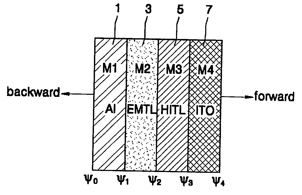
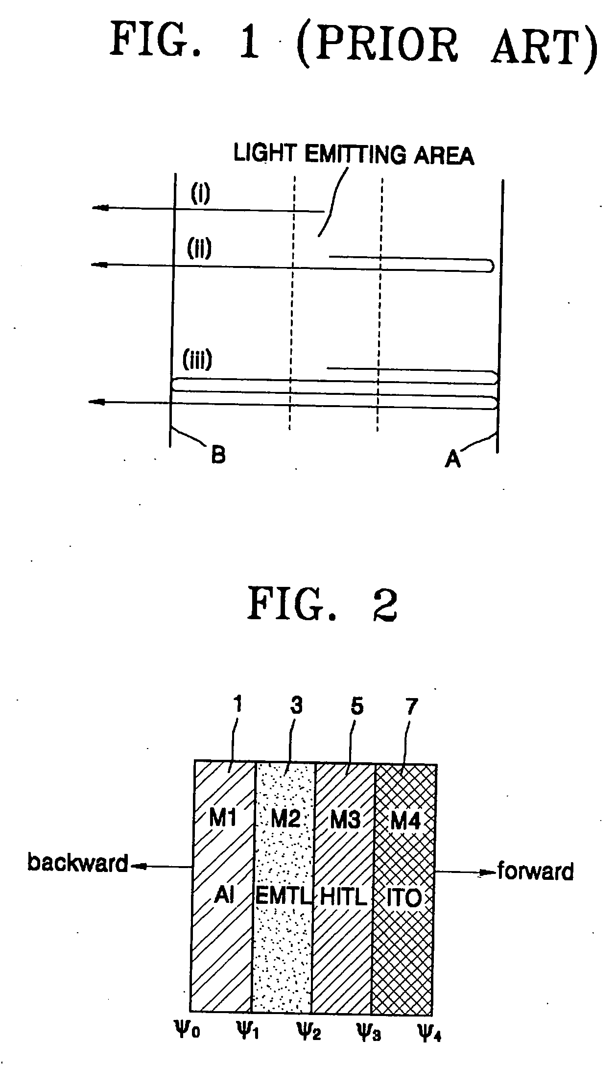
[0040] With reference not to FIG. 2, a schematic diagram of an organic electroluminescence device according to an embodiment of the present invention is illustrated. The organic electroluminescence device includes a second electrode 1, an EMTL 3, an HITL 5, and a first electrode 7. In certain embodiments, the EMTL 3 may include an electron transport layer (ETL), an emitting layer (EML), and an optional electron injection layer (EIL). In certain embodiments, the HITL 5 may include a hole transport layer (HTL) and a hole injection layer (HIL). For clarity FIG. 2 does not show a substrate.

[0041] Organic electroluminescence devices are classified into forward emitting types and backward emitting types depending on the emitting method. The organic electro...


PUM

PropertyMeasurementUnit
refractive indexaaaaaaaaaa
thicknessaaaaaaaaaa
wavelengthaaaaaaaaaa

Abstract

An organic electroluminescence device is described and includes a transparent substrate with a first electrode formed on the top surface of the transparent substrate in a predetermined pattern. The first electrode is transparent. An organic layer includes a hole injecting layer, a hole transporting layer, an emitting layer, and an electron transporting layer. They are sequentially stacked on the top surface of the first electrode. A second electrode is formed on the top surface of the organic layer in a predetermined pattern. The distance from the top surface of the hole transporting layer to the bottom surface of the second electrode ranges from about 350 Å to about 450 Å such that the color purity and brightness of blue light is optimized. Accordingly, the organic electroluminescence device increases the color purity and brightness of blue light, thereby providing an image having excellent picture quality.

Description

BACKGROUND OF THE INVENTION [0001] 1. Field of the Invention [0002] The present invention relates to an organic electroluminescence device, and more particularly, to an organic electroluminescence device capable of increasing color purity and brightness. [0003] 2. Description of the Related Art [0004] Electroluminescence display devices are generally classified into inorganic electroluminescence devices and organic electroluminescence devices depending on the materials used for the emitting layer. [0005] In organic electroluminescence devices, electrons and holes are combined in the emitting layer, to form excitons. Excitons in an excited state move to a ground state and transmit energy to fluorescent molecules in the emitting layer. The fluorescent molecules emit light and thereby form an image. [0006] Organic electroluminescence devices have a higher brightness, require lower voltages, and have faster response times than inorganic electroluminescence devices. Organic electrolumine...

Claims


Application Information

Patent Timeline
Patent Type & Authority Applications(United States)
IPC IPC(8): H05B33/26H01L51/50H01L51/52
CPCH01L51/5048H01L51/5096H01L51/5262Y10T428/24942Y10S428/917Y10T428/26H01L2251/558H10K50/14H10K50/18H10K50/85H10K2102/351H05B33/26
Inventor SONG, SU-BINOH, JUN-SIKLEE, HAN-JUJU, SANG-HYUN
Owner SAMSUNG DISPLAY CO LTD
Features
  • R&D
  • Intellectual Property
  • Life Sciences
  • Materials
  • Tech Scout
  • Unparalleled Data Quality
  • Higher Quality Content
  • 60% Fewer Hallucinations
Learn More