Plasma display device

a display device and plasma technology, applied in the direction of gas discharge vessels/containers, electric discharge tubes, instruments, etc., can solve the problems of unstable address scanning, uncertain selective discharge, and higher cost, and achieve the effect of speeding up address scanning without damaging the stability of address scanning

Inactive Publication Date: 2005-12-01
PANASONIC CORP
View PDF11 Cites 29 Cited by
  • Summary
  • Abstract
  • Description
  • Claims
  • Application Information

AI Technical Summary

Benefits of technology

[0015] It is an object of the present invention to provide a plasma display device and a driving method therefor which are capable of speeding up address scanning without damaging the stability of the address scanning.

Problems solved by technology

If the pulse width of a scanning pulse is simply narrowed down to limit the increased addressing period, a selective discharge becomes uncertain due to a delayed discharge and the like.
This address scanning technique requires a column electrode driving circuit for each of the column electrode groups which are divided into an upper and a lower section, resulting in a higher cost.
Also, a problem still remains unchanged in regard to the stability of the address discharge because the address discharge is more difficult to occur in display lines which are scanned in later turns, as compared with the display line which is scanned first.

Method used


Image

  • Plasma display device
  • Plasma display device
  • Plasma display device

Examples


Embodiment Construction

[0035] In the following, embodiments of the present invention will be described in detail with reference to the drawings.

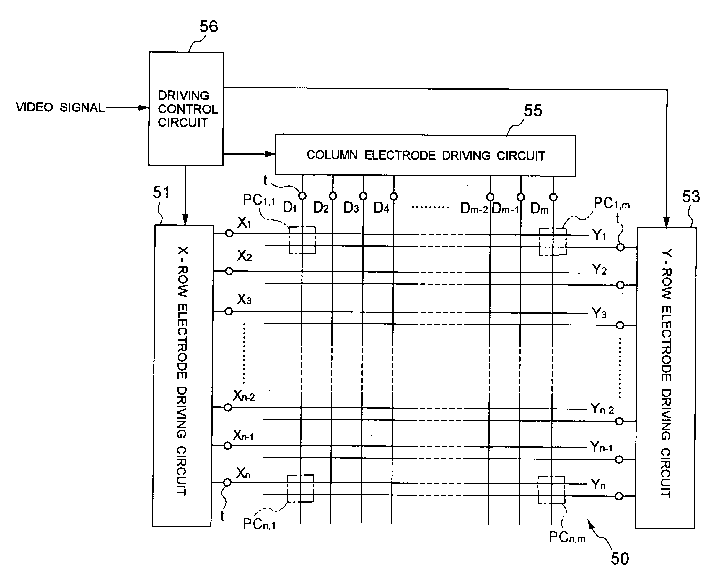
[0036]FIG. 4 is a diagram generally showing the configuration of a plasma display device according to the present invention.

[0037] As shown in FIG. 4, the plasma display device comprises a PDP 50 as a plasma display panel, an X-row electrode driving circuit 51, a Y-row electrode driving circuit 53, a column electrode driving circuit 55, and a driving control circuit 56.

[0038] The PDP 50 is formed with column electrodes D1-Dm respectively extending in a vertical direction of a two-dimensional display screen, and row electrodes X1-Xn and row electrodes Y1-Yn respectively extending in the horizontal direction of the two-dimensional display screen. In this event, row electrode pairs (Y1, X1), (Y2, X2), (Y3, X3), . . . , (Yn, Xn), which form pairs with adjacent ones to each other, form a first display line to an n-th display line on the PDP 50. At the intersection o...


PUM


Abstract

A plasma display device having a plasma display panel in which, each display cell contains a magnesium oxide layer including magnesium oxide crystals that are excited by an electron beam to emit cathode luminescence light having a peak in a wavelength range of 200 to 300 nm. In an addressing period, a row electrode driving circuit applies a scanning pulse to one row electrodes of row electrode pairs in turn, while a column electrode driving circuit supplies column electrodes with data pulses corresponding to one row electrode which is applied with the scanning pulse.

Description

BACKGROUND OF THE INVENTION [0001] 1. Field of the Invention [0002] The present invention relates to a plasma display device in which a plasma display panel is used. [0003] 2. Description of the Related Art [0004] For driving a plasma display panel (PDP), a one-field display period is composed of a plurality of sub-fields, each including an addressing period and a sustain period, to display images at multiple gradation levels. In a gradation display method, when the number of display lines is increased for a higher definition or when the number of sub-fields is increased for an increased number of gradation levels, the proportion of the addressing period relatively increases in the one-field display period. If the pulse width of a scanning pulse is simply narrowed down to limit the increased addressing period, a selective discharge becomes uncertain due to a delayed discharge and the like. To solve this problem, a driving method, which divides column electrodes of a PDP into two gro...

Claims


Application Information

Patent Timeline
Patent Type & Authority Applications(United States)
IPC IPC(8): G09G3/20G09G3/288G09G3/291G09G3/293G09G3/294G09G3/298H01J11/14H01J11/22H01J11/24H01J11/34H01J11/40
CPCG09G3/2932H01J11/40H01J11/12G09G3/291
Inventor TOKUNAGA, TSUTOMUNISHIMURA, MASARUSAKATA, KAZUAKIHIROTA, ATSUSHILIN, HAI
Owner PANASONIC CORP
Why Eureka
Try Eureka