Managing communication bandwidth in co-verification of circuit designs

Active Publication Date: 2006-02-16
SIEMENS PROD LIFECYCLE MANAGEMENT SOFTWARE INC
View PDF7 Cites 10 Cited by
  • Summary
  • Abstract
  • Description
  • Claims
  • Application Information

AI Technical Summary

Benefits of technology

[0011] Once the signals to be included in a channel have been selected, then the components responsible for producing those communication signals can be located proximal to each other within the emulator. More particularly, once the communication signals to be included in a channel have been selected, the circuit components that will send or receive those signals are ide

Problems solved by technology

Some modern electronic circuit designs, such as the designs of electronic circuits integrated onto a metal substrate (often referred to as “integrated circuits” or “IC chips”), have become extremely complex.
As a result, various techniques have been developed to verify that circuit designs will operate as desired before they are implemented in an expensive ma

Method used


Image

  • Managing communication bandwidth in co-verification of circuit designs
  • Managing communication bandwidth in co-verification of circuit designs
  • Managing communication bandwidth in co-verification of circuit designs

Examples


Embodiment Construction

[0022] Operating Environment

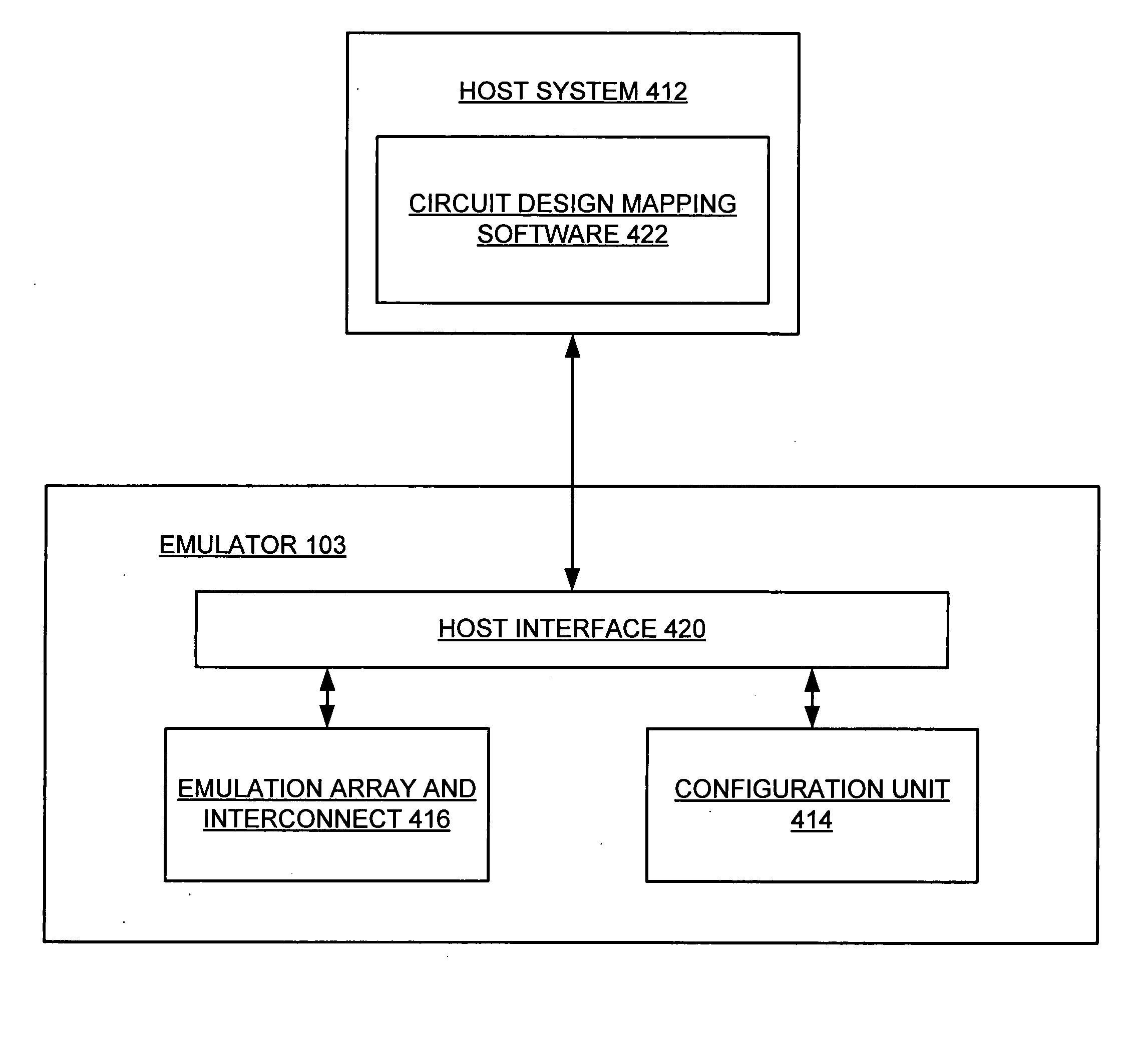
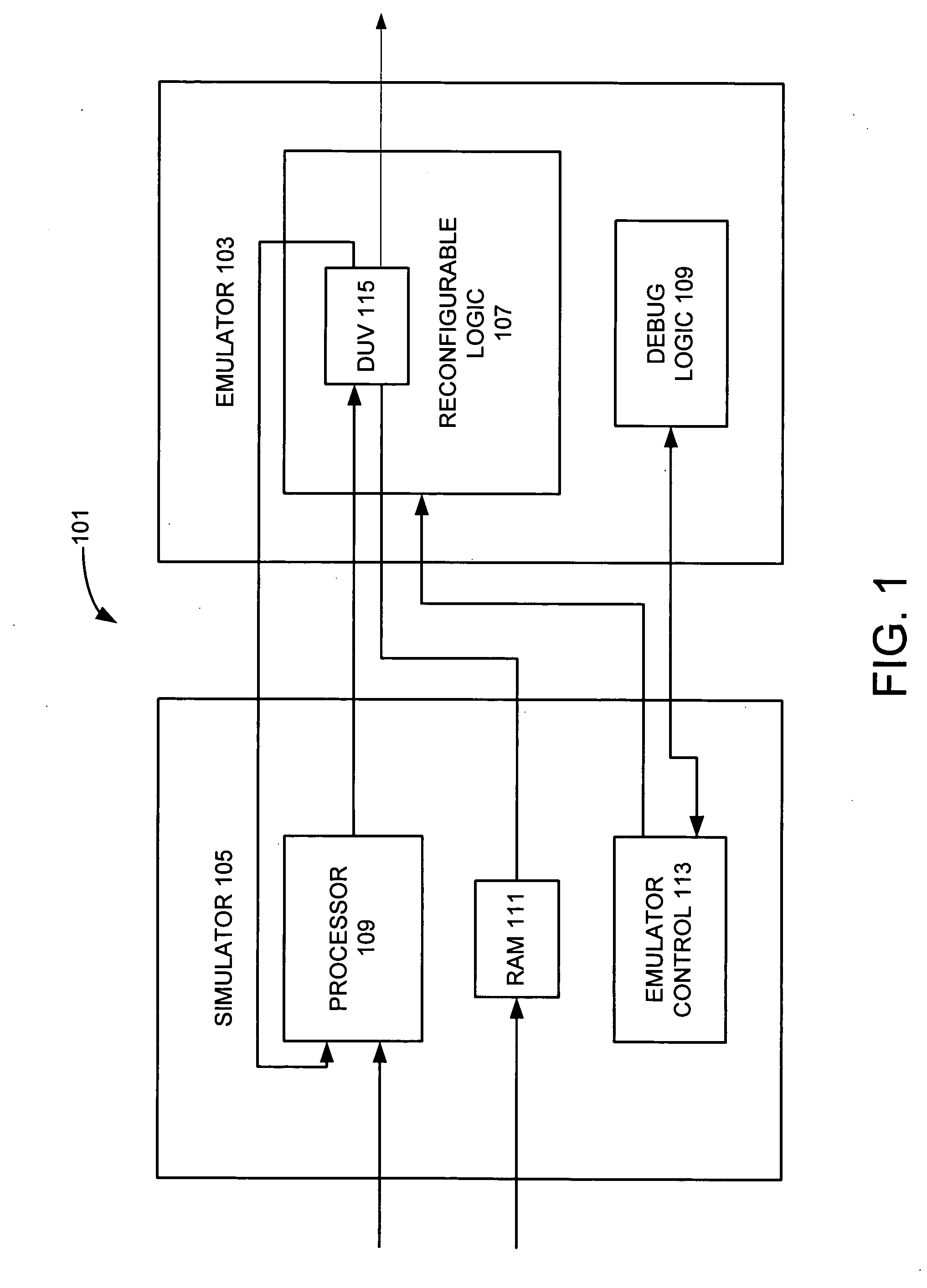
[0023]FIG. 1 illustrates a high level view of a system 101 for verifying a circuit design.

[0024] The system 101 includes an emulator 103 and a simulator 105. The emulator 103 includes a group of reconfigurable logic devices 107, such as field programmable gate arrays (FPGA). The emulator 103 may also include one or more debugging logic devices 109, for debugging problems in the reconfigurable logic devices 107.

[0025] It should be appreciated that the system 101 can be employed to verify any desired type of circuit design. For example, various embodiments of the system 101 can be employed to test a design of an entire device, such as a microprocessor or integrated circuit memory. Some embodiments of the invention also may be employed to test a design for only a portion of a device, such as a register or other memory structure serving as a component in a larger device. Still further, various embodiments of the invention may be used to verify a circuit de...


PUM


Abstract

Related communication signals between a simulator and an emulator are organized into logical channels. The signals in each channel are then be transmitted only as needed, reducing the use of the communication pathways between the simulator and the emulator. Further, the circuit components that will receive the communication signals to be shared on a channel are be physically located close together within the emulator, thereby reducing the time required to select and enable components of the emulator to receive the signals sent by the simulator. Similarly, emulator components that send communication signals to be shared on a channel are physically located close together within the emulator, thereby reducing the time required to select and enable components of the emulator to send these signals to the simulator.

Description

RELATED APPLICATIONS [0001] This application is a continuation-in-part of U.S. Provisional Patent Application No. 60 / 651,456, filed on Jul. 6, 2004, entitled “Managing Communication Bandwidth In Co-Verification Of Circuit Designs” and naming Nicolas Chaumont et al. as inventors, which application is incorporated entirely herein by reference.FIELD OF THE INVENTION [0002] The present invention relates to the management of communication bandwidth in the co-verification of circuit designs, such as integrated circuit designs. Various aspects of the invention more particularly relate to the use of different communication protocols for different groups of communication signals during the co-verification of an integrated circuit design. BACKGROUND OF THE INVENTION [0003] Some modern electronic circuit designs, such as the designs of electronic circuits integrated onto a metal substrate (often referred to as “integrated circuits” or “IC chips”), have become extremely complex. As a result, va...

Claims


Application Information

Patent Timeline
IPC IPC(8): G06F9/455G06G7/62
CPCG06F17/5054G06F30/34
Inventor CHAUMONT, NICOLASBRAULT, JEAN-MARC
Owner SIEMENS PROD LIFECYCLE MANAGEMENT SOFTWARE INC
Why Eureka
Try Eureka