Terahertz interconnect system and applications

a technology of terahertz interconnection and interconnection system, applied in the field of terahertz interconnection, can solve the problems of increasing the amount and speed of data transfer in communication and computing system, reducing the cost of rf interconnect design and manufacture, and increasing the cost of high signal frequency rf lines. , to achieve the effect of increasing performan

Inactive Publication Date: 2006-02-23
UNIV OF COLORADO THE REGENTS OF
View PDF61 Cites 171 Cited by
  • Summary
  • Abstract
  • Description
  • Claims
  • Application Information

AI Technical Summary

Problems solved by technology

Increased amounts and speed of data transfer in communication and computing systems pose a challenge to the current state of device technology.
However, RF interconnects use large antennae and / or waveguides on or connected to chips, thus requiring valuable on-chip and device “real estate.” RF interconnects are limited in data transfer speed due to the use of radio frequencies.
Furthermore, It is submitted that the design and manufacture of such RF lines for high signal frequencies is an expensive part of prior art RF interconnection design.
Other researchers have suggested the use of optical signals as an alternative to electrical signals in providing inter- and intra-chip connections.1 For instance, parallel fiber-optic interconnects which are edge-connected to semiconductor devices have been developed for use within systems with a large number of electronic components (e.g., computers).2 Although optical interconnect technology promises the possibility of higher rate data transfer than electrical interconnects, optical interconnect technology, as heretofore suggested, is still cost prohibitive in comparison.
Such hardwired connections add parasitic capacitance, inductance, and resistance, which seriously degrade data transmission at high data bandwidths.
Thus, the cost and performance limitations of electrical interconnects are compounded as circuits are made to operate at increasingly high frequencies.
At high frequencies, electrical interconnects are limited in connection distance and require large amounts of power as well as signal reconditioning.
First issue is the relative change in material properties, such as refractive index and electromagnetic radiation propagation speed, over the bandwidth of the signal.
A second, and perhaps more significant, issue is the relative difference in wavelength over the bandwidth of the signal.
This enormous range in wavelength makes it difficult to design electrical transmission paths which will work efficiently over the entire bandwidth range.
It is submitted, however, that GaAs-based MIMICs are complex devices which require expensive epitaxial growth techniques in the fabrication.
Applicants submit that epitaxial growth techniques are expensive and severely limit the integration of devices with different epitaxial layer structures.
However, Applicants submit that ultrashort pulse generation, such as that disclosed in Duling, require complex systems such as femtosecond lasers that are impractical to use as a replacement for local electrical interconnects.

Method used


Image

  • Terahertz interconnect system and applications
  • Terahertz interconnect system and applications
  • Terahertz interconnect system and applications

Examples


Embodiment Construction

[0063] The following description is presented to enable one of ordinary skill in the art to make and use the invention and is provided in the context of a patent application and its requirements. Various modifications to the described embodiments will be readily apparent to those skilled in the art and the generic principles herein may be applied to other embodiments. Thus, the present invention is not intended to be limited to the embodiment shown but is to be accorded the widest scope consistent with the principles and features described herein.

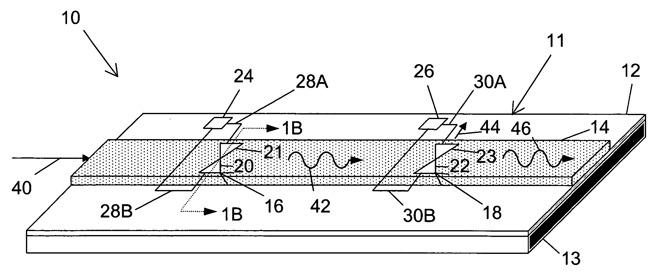
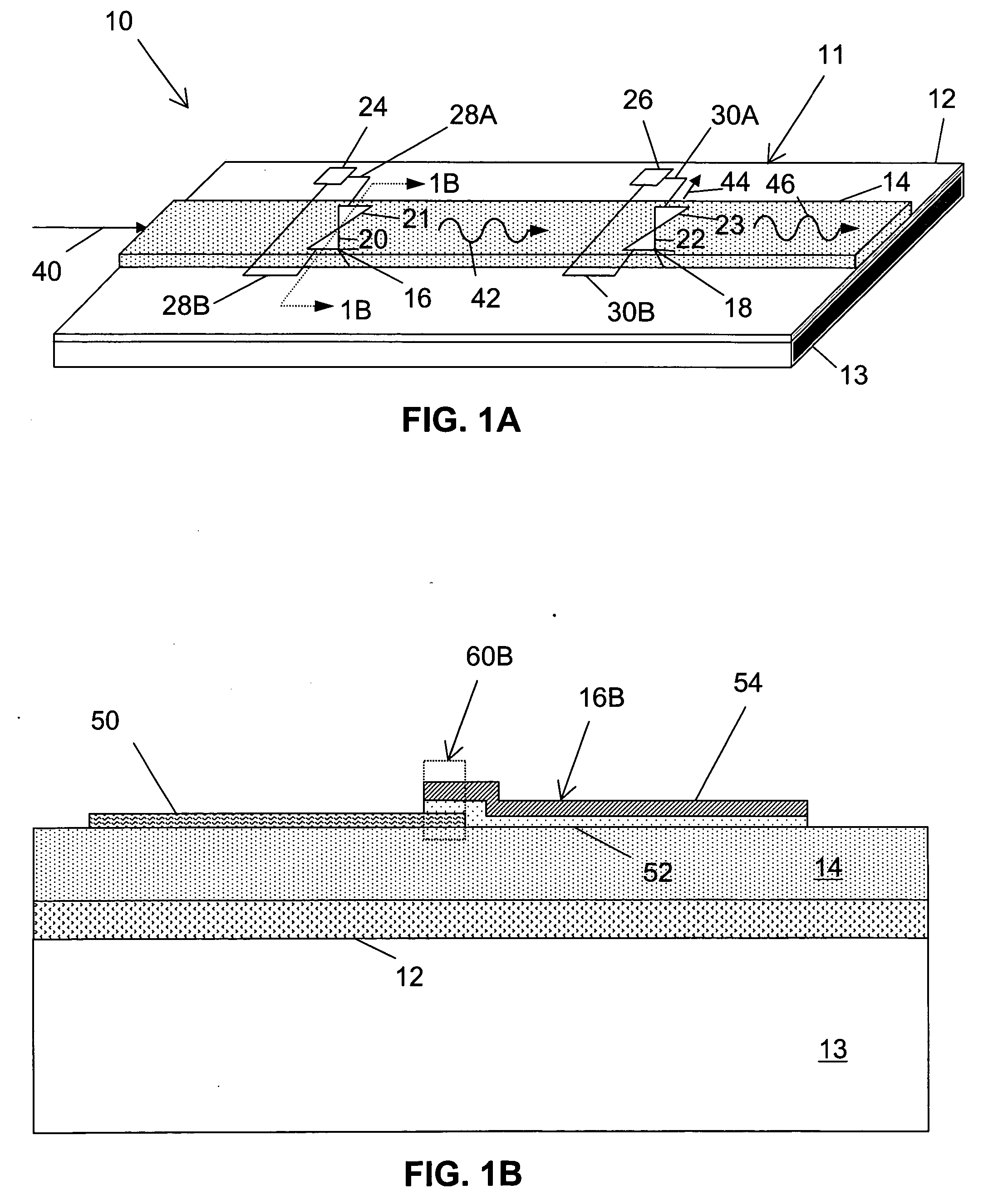
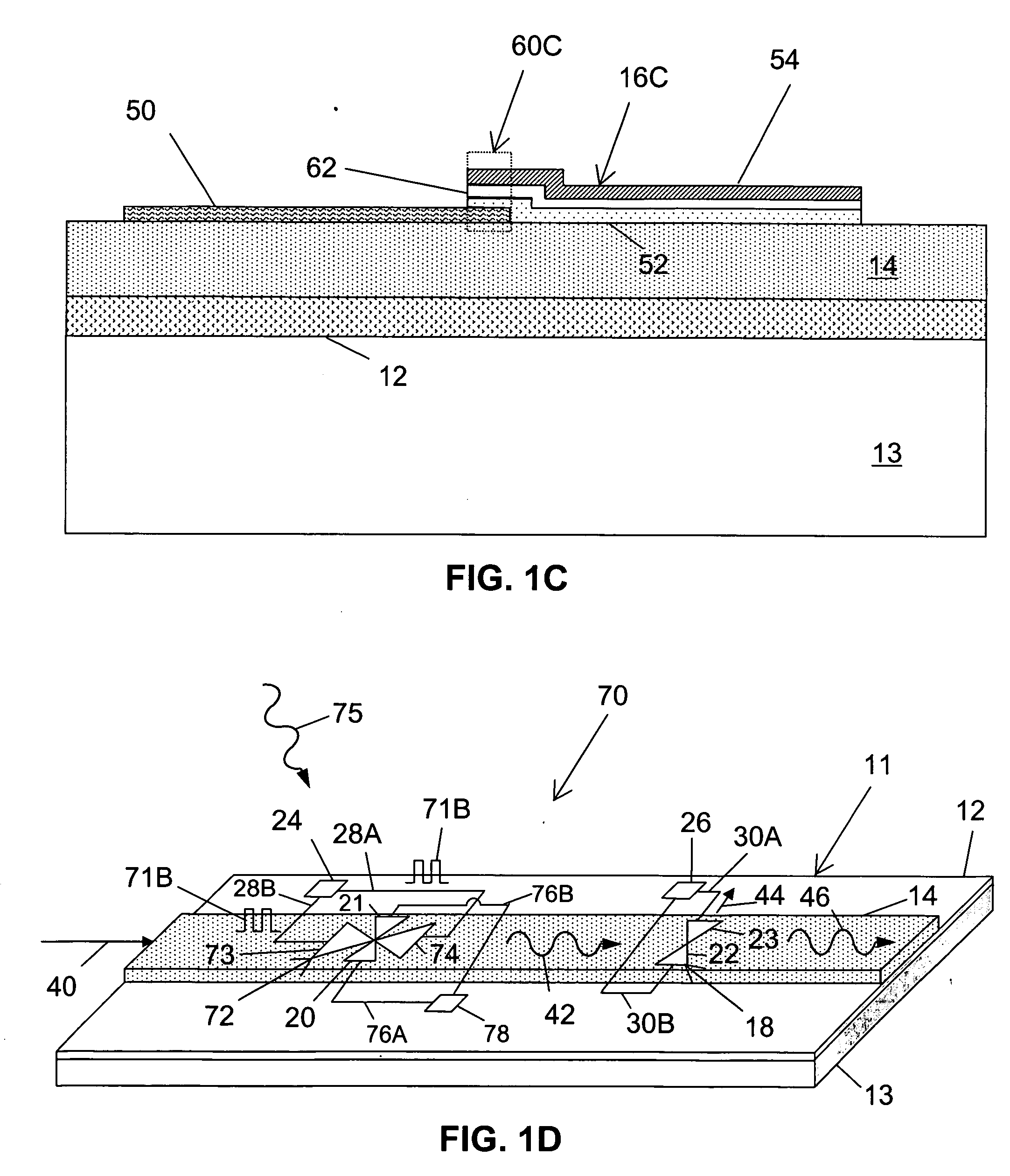
[0064] As described in the Background section, there is a growing need for high speed interconnection between devices over short distances, such as between racks, boards, chips, as well as between components located on a single chip. These interconnection arrangements must be capable of high speed transmission of data and should be low cost. The interconnection arrangements and systems need to be competitive and compatible with current sta...


PUM


Abstract

An assembly includes a first electrical circuitry for providing a first electrical signal containing data and a transmitting arrangement, connected with the first electrical circuitry, for receiving the first electrical signal and for converting the first electrical signal into an electromagnetic signal containing at least a portion of the data. The electromagnetic signal has a carrier frequency greater than 300 GHz. The assembly also includes a receiving arrangement for receiving the electromagnetic signal and for converting the electromagnetic signal into a second electrical signal containing at least some of the portion of the data, and a second electrical circuitry connected with the receiving arrangement and configured for receiving the second electrical signal.

Description

RELATED APPLICATION [0001] The present application is a continuation of copending application Ser. No. 10 / 462,491, filed on Jun. 14, 2001; which is a continuation-in-part application Ser. No. 10 / 337,427, filed on Jan. 6, 2003; which is a continuation-in-part of applications 1) Ser. No. 09 / 860,988, filed May 21, 2001 and issued as U.S. Pat. No. 6,534,784, 2) Ser. No. 09 / 860,972, filed May 21, 2001 and issued as U.S. Pat. No. 6,564,185, 3) Ser. No. 10 / 103,054, filed on Mar. 20, 2002, and 4) Ser. No. 10 / 140,535, filed May 6, 2002. All of the aforementioned patent applications and patents are incorporated herein by reference in their entirety.BACKGROUND OF THE INVENTION [0002] The present invention relates generally to electronic devices. More particularly, the present invention relates to interconnection of electronic devices at carrier frequencies in a range from a few gigahertz to several hundreds of terahertz, and more specifically to terahertz interconnection of electronic devices....

Claims


Application Information

Patent Timeline
Patent Type & Authority Applications(United States)
IPC IPC(8): H01L29/06G02B6/122G02B6/42G11C7/00H01L23/48H01L31/0336
CPCB82Y10/00B82Y20/00H01L2924/0002G02B6/12004G02B6/1226G02B6/34G02B6/4201G02B6/4292G02B6/43G02B2006/12123G02B2006/1213G02B2006/12142H01L23/48H01L25/0657H01L31/035236H01L31/06H01L31/101H01L2225/06513H01L2924/3011Y02E10/50H01L2225/06534H01L2924/00G02B6/4279
Inventor ESTES, MICHAEL J.MODDEL, GARRET
Owner UNIV OF COLORADO THE REGENTS OF
Why Eureka
Try Eureka