
Plasma display device and driving method thereof

a technology of a display device and a driving method, which is applied in the direction of gas discharge vessels/containers, auxillary electrodes, instruments, etc., can solve the problems of insufficient discharge, distorted waveforms alternately applied to the x electrode and the y electrode, and insufficient discharg

Inactive Publication Date: 2006-03-23
SAMSUNG SDI CO LTD
View PDF8 Cites 12 Cited by
  • Summary
  • Abstract
  • Description
  • Claims
  • Application Information

AI Technical Summary

Benefits of technology

The present invention provides a plasma display device and a driving method that can prevent insufficient discharges. This is achieved by gradually increasing and decreasing the voltage at the electrodes during the reset and address periods, and alternately applying a sustain discharge pulse to the electrodes. The driving circuit includes a first electrode driver and a third electrode driver, which gradually increase and decrease the voltage at the first electrode, respectively. The third electrode driver gradually decreases the voltage at the third electrode by turning on a fourth switch after the voltage at the third electrode is gradually increased. This invention improves the reliability and stability of plasma display devices.

Problems solved by technology

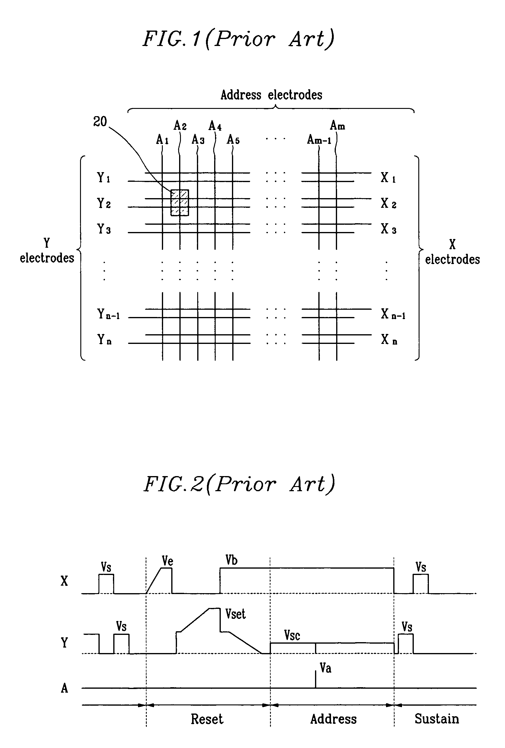
However, in the conventional plasma display device, an insufficient discharge may occur since insufficient priming particles may be generated in the selected discharge cells when applying a first sustain pulse after the address period.
Accordingly, the X and Y electrode driving circuits do not have matching impedance, the waveform alternately applied to the X electrode and the Y electrode may be distorted in the sustain discharge period, and an insufficient discharge may occur.

Method used


Image

  • Plasma display device and driving method thereof
  • Plasma display device and driving method thereof
  • Plasma display device and driving method thereof

Examples


Embodiment Construction

[0033] Exemplary embodiments of the present invention will hereinafter be described in detail with reference to the accompanying drawings.

[0034] In the following detailed description, only certain exemplary embodiments of the present invention have been shown and described, simply by way of illustration. As those skilled in the art would realize, the described embodiments may be modified in various different ways, all without departing from the spirit or scope of the present invention. Accordingly, the drawings and description are to be regarded as illustrative in nature and not restrictive. Like reference numerals designate like elements throughout the specification. As used herein, erase, erased, and erasing do not necessarily require removal of all traces of the thing being erased.

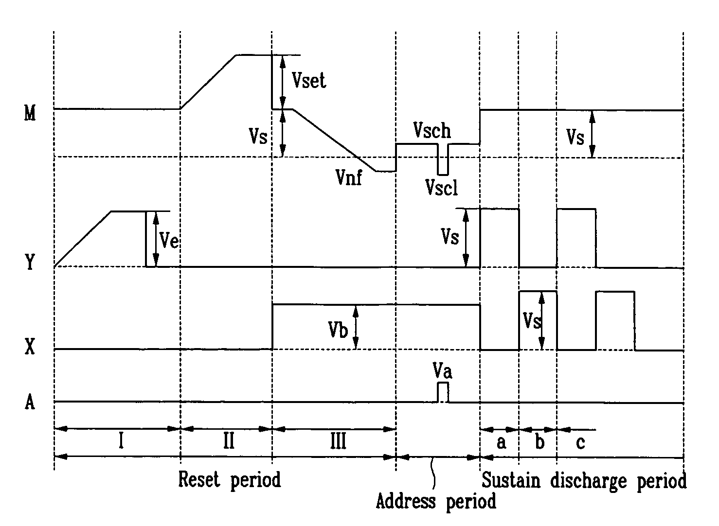
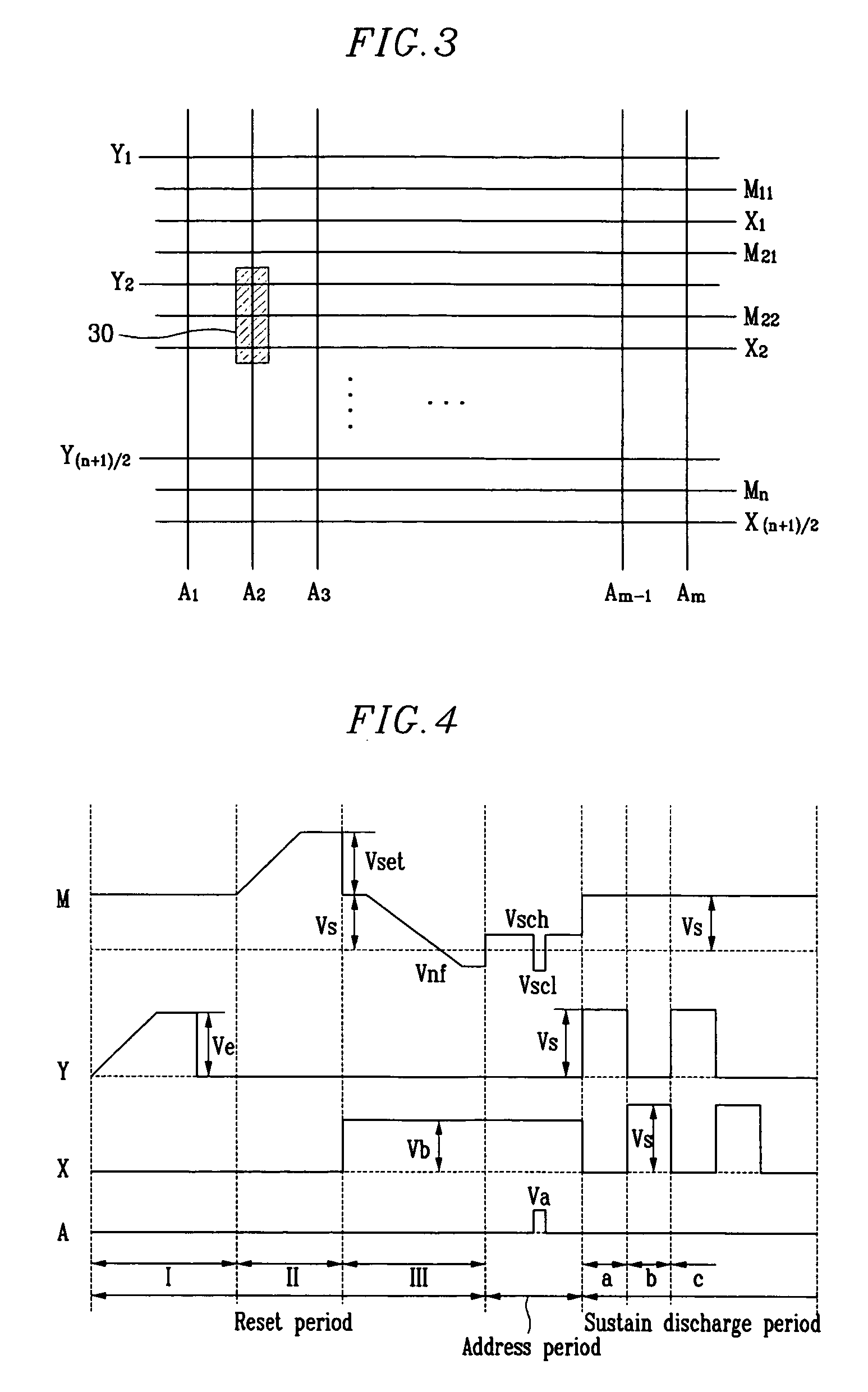
[0035] A plasma display device according to an exemplary embodiment of the present invention will now be described with reference to FIG. 3 and FIG. 4.

[0036]FIG. 3 shows an electrode arrangement diag...


PUM


Abstract

In a plasma display device and driving method thereof, middle electrodes are formed between X electrodes for receiving a sustain pulse voltage and Y electrodes. A reset waveform and a scan pulse voltage are applied to the middle electrodes. A short-gap discharge is performed between the X electrode and the middle electrode in the earlier stage of a sustain discharge period, and a long-gap discharge is normally performed between the X electrode and the Y electrode after the earlier stage of the sustain discharge period, thereby performing stable discharge. Further, the number of switches of the M electrode driver may be reduced by floating the M electrode and applying a rising ramp waveform to the Y electrode in the reset period, thereby increasing the voltage at the M electrode.

Description

CROSS-REFERENCE TO RELATED APPLICATION [0001] This application claims priority to and the benefit of Korean Patent Application No. 10-2004-0075433, filed on Sep. 21, 2004, which is hereby incorporated by reference for all purposes as if fully set forth herein. BACKGROUND OF THE INVENTION [0002] 1. Field of the Invention [0003] The present invention relates to a plasma display device. [0004] 2. Discussion of the Background [0005] Generally, a plasma display device utilizes a plasma panel display (PDP) to display letters or images by plasma generated by a gas discharge, and the PDP may have millions of pixels arranged in a matrix format depending on its size. The PDP may be a direct current (DC) PDP or an alternating current (AC) PDP according to applied driving voltage waveforms and discharge cell structures. [0006] The DC PDP's electrodes are exposed in a discharge space in which current flows while a voltage is applied. Hence, a resistor is provided to control the current. On the o...

Claims


Application Information

Patent Timeline
Patent Type & Authority Applications(United States)
IPC IPC(8): G09G3/28G09G3/288G09G3/20G09G3/291G09G3/292G09G3/293G09G3/294G09G3/296G09G3/298H01J11/22H01J11/24H01J11/28H01J11/34
CPCG09G3/291G09G3/2927G09G2320/0228G09G3/2986G09G2310/066G09G3/2965G09G3/292G09G3/293G09G3/296
Inventor KIM, JOON-YEONKIM, JEONG-NAMKIM, GAB-SICKCHO, SUNG-CHUN
Owner SAMSUNG SDI CO LTD
Learn More