

Digital-to-analog converting circuit and display device using same
- Summary
- Abstract
- Description
- Claims
- Application Information
AI Technical Summary
Benefits of technology
Problems solved by technology
Method used
Image

Examples
Embodiment Construction
[0106] Embodiments of the present invention will now be described with reference to the drawings.
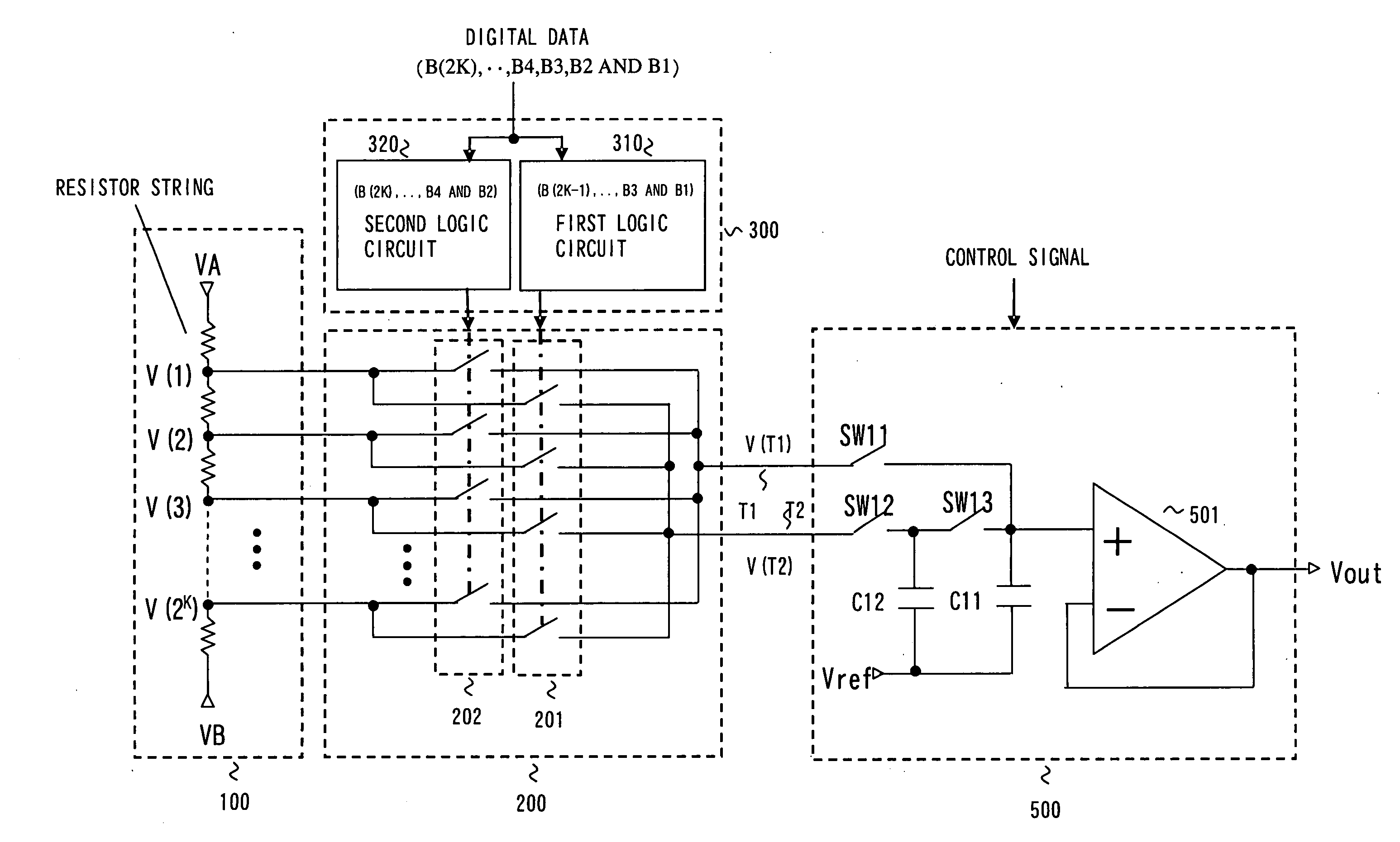
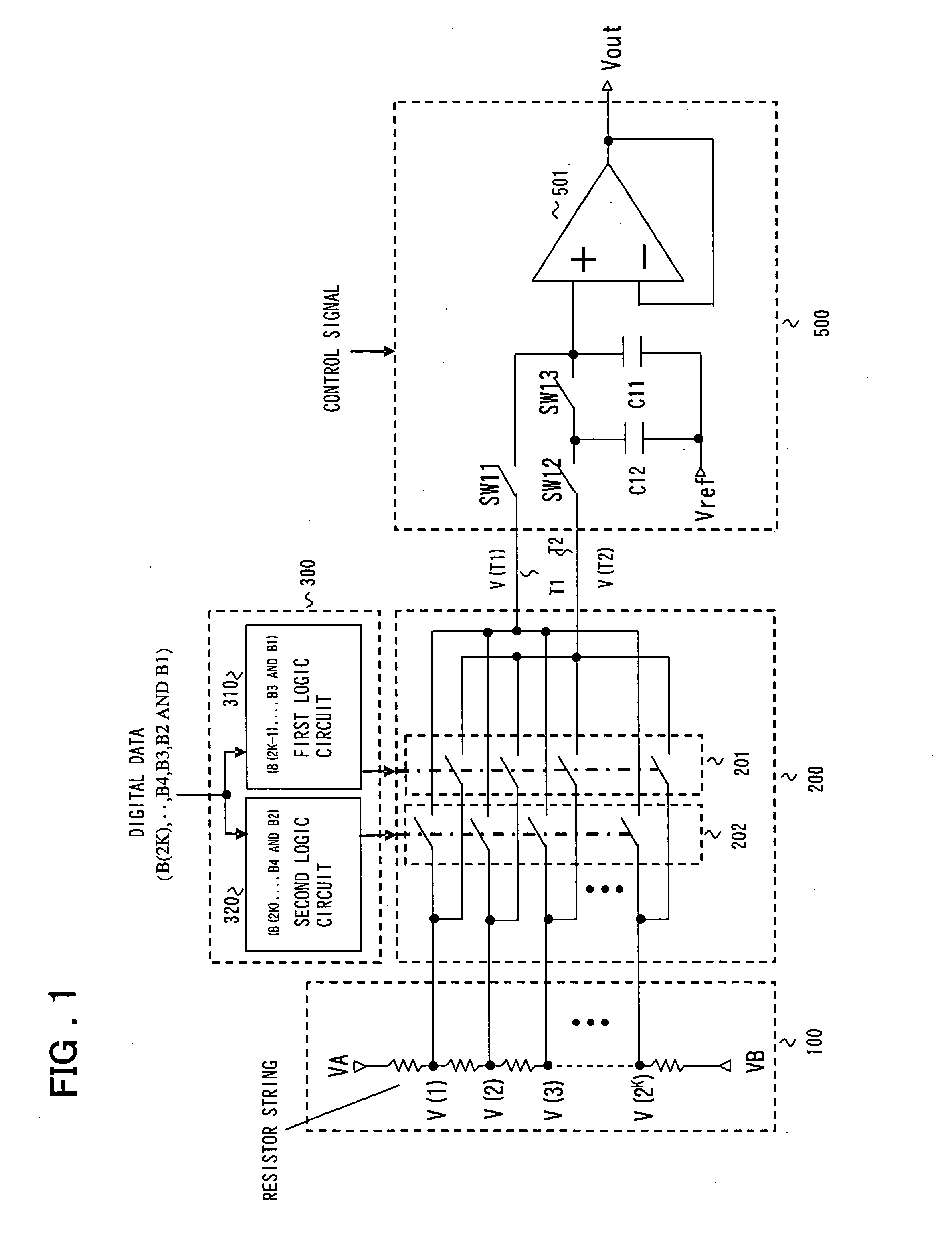
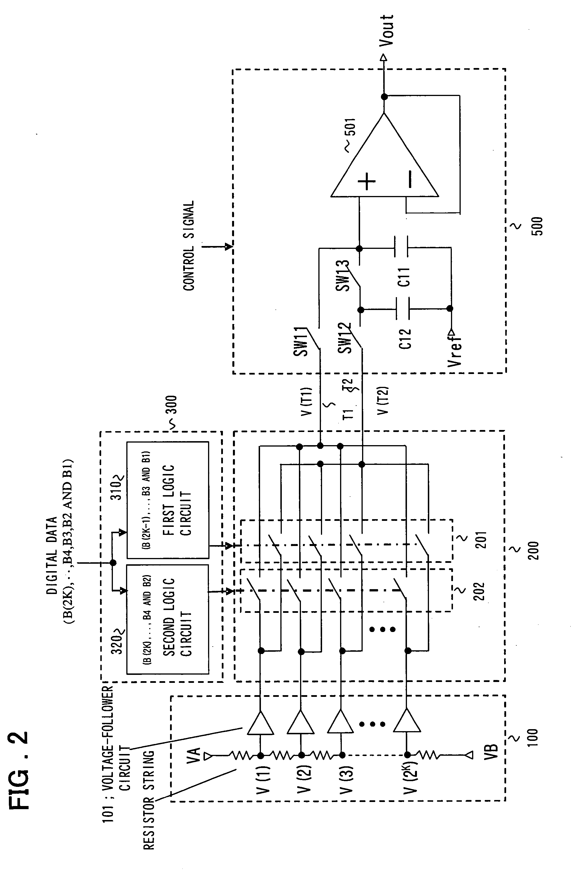
[0107]FIG. 1 is a diagram illustrating the structure of a digital-to-analog converter (DAC) according to a first embodiment of the present invention. As shown in FIG. 1, the DAC according to the first embodiment includes a reference voltage generating circuit 100 for generating 2K-number of reference voltages [V(1), V(2), . . . , and V(2K)]; a logic circuit 300, which receives input of a 2K-bit digital signal [B(2K), B(2K−1), . . . , B3, B2 and B1], for outputting logic values; a switch group 200 for selecting two identical or different reference voltages from among the 2K-number of reference voltages based upon the logic values, and outputting these voltages to terminals T1 and T2; and an operational amplifier circuit 500 for amplifying and outputting a voltage obtained by internally dividing (interpolating) or externally dividing (extrapolating) the voltages of the terminals T1 and T2...
PUM
 Abstract
Description
Claims
Application Information