Electronic device having smaller number of drive chips

Active Publication Date: 2017-06-29
TCL CHINA STAR OPTOELECTRONICS TECH CO LTD
View PDF4 Cites 6 Cited by
  • Summary
  • Abstract
  • Description
  • Claims
  • Application Information

AI Technical Summary

Benefits of technology

[0016]The electronic device of the present invention has smaller number of drive chips a

Problems solved by technology

However, the number of gate drive chips and source drive chips required are also gr

Method used


Image

  • Electronic device having smaller number of drive chips
  • Electronic device having smaller number of drive chips
  • Electronic device having smaller number of drive chips

Examples


first embodiment

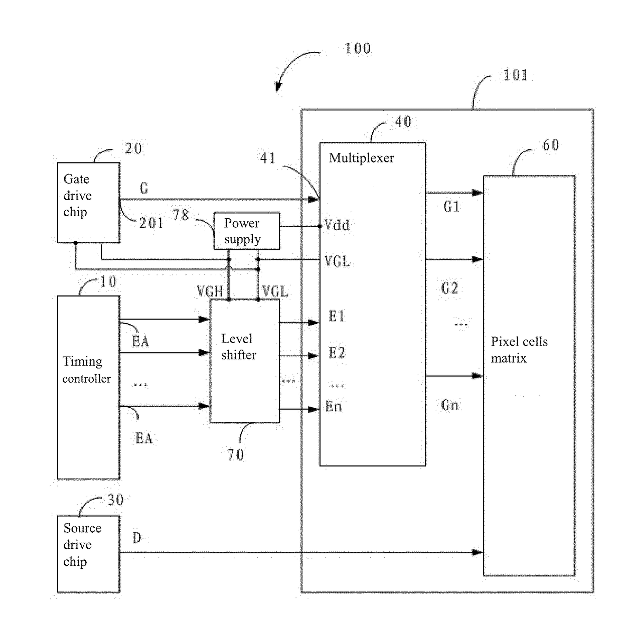
[0031]Wherein, as shown in the FIG. 1, in the present invention, the timing controller 10 includes a plurality of enable signal output ends EA. Each enable signal output end EA of the timing controller 10 is connected respectively to the enable ends E1˜En of the multiplexer 40 to control the enable signal output end EA to output enable signals to the enable ends E1˜En of the multiplexer 40.

[0032]Wherein, as shown in the FIG. 1, in the present embodiment, the electronic device 100 also includes a level shifter 70. The level shifter 70 is connected between the enable signal output ends EA of the timing controller 10 and the enable ends E1˜En of the multiplexer 40 to output each boosted enable signal of the enable signal output EA of the timing controller 10 to the corresponding enable end of the multiplexer 40.

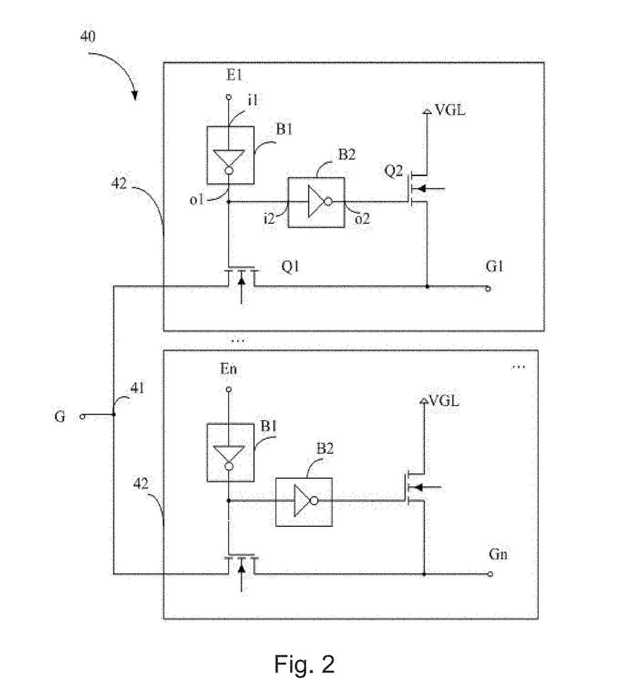
[0033]Wherein, the multiplexer 40 includes a plurality of path selecting circuits, each of which comprises a first NMOS and a first boost inverter; the first boost inverter comp...

second embodiment

[0046]Please refer to FIG. 5, in the second embodiment, the multiplexer 40 and the pixel cells matrix 60 and the level shifter 70 are all mounted on the array substrate 101.

third embodiment

[0047]Please refer to FIG. 6, in the third embodiment, the electronic device 100 also includes a shift register 90. In the present embodiment, the timing controller 10 only includes an enable signal output end E to output enable signals. The level shifter 70 is connected to the enable signal output end E to boost the enable signal output thereof. The shift register 90 is connected between the level shifter 70 and enable ends E1˜En of the multiplexer 40 to sequentially apply the boosted enable signals by the level shifter 70 onto the enable ends E1˜En of the multiplexer 40. In this way, the enable ends E1˜En of the multiplexer 40 could sequentially receive the enable signals and sequentially output the scanning signals by the signal output ends G1˜Gn.

[0048]Wherein, in the third embodiment, the multiplexer 40, the pixel cells matrix 60, the level shifter 70 and the shift register 90 are all mounted on the array substrate 101.

[0049]Wherein, the electronic device 100 might be a LCD TV, ...


PUM


Abstract

The present invention provides an electronic device (100) having smaller number of drive chips and including a timing controller (10), a gate and a source drive chips (20, 30), a pixel cells matrix (60) and a multiplexer (40). The multiplexer (40) includes a plurality of first signal outputs connected to the pixel cells matrix (60). The timing controller (10) might generate enable signals for the multiplexer (40). In this way, the multiplexer (40) could output scan signals to the pixel cells matrix by a corresponding signal end. The number of the drive chips could be reduced by the present invention.

Description

FIELD OF THE INVENTION[0001]The present invention relates to electronic devices, and more particularly to electronic devices with display function.BACKGROUND OF THE INVENTION[0002]At present, LCD (liquid crystal display) monitors and other display devices are already very common. Due to the need for large-size screen, one of development trends of the LCD display devices is large-scale. However, the number of gate drive chips and source drive chips required are also greatly increased in such size-enlarged screens, which could result in increased cost.SUMMARY OF THE INVENTION[0003]An object of the present invention is to provide an electronic device having smaller number of drive chips to drive large-size screens.[0004]The present invention provides an electronic device having smaller number of drive chips, the electronic device comprises a timing controller, a gate drive chip, a source drive chip and a pixel cells matrix; the gate drive chip comprises at least one drive signal output...

Claims


Application Information

Patent Timeline
IPC IPC(8): G09G3/36
CPCG09G3/3674G09G3/3611G09G3/3685G09G3/2096G09G2310/0278G09G2310/0289
Inventor KUO, PING-SHENGHWANG, TAI-JIUN
Owner TCL CHINA STAR OPTOELECTRONICS TECH CO LTD
Why Eureka
Try Eureka