Liquid crystal display device and method for manufacturing the same
- Summary
- Abstract
- Description
- Claims
- Application Information
AI Technical Summary
Benefits of technology
Problems solved by technology
Method used
Image
Examples
first embodiment
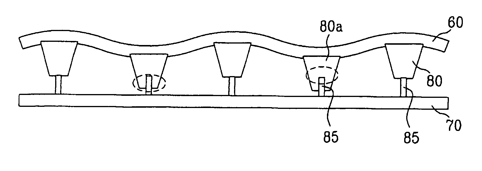
[0053]FIGS. 6A and 6B are sectional views illustrating a state before and after upper and lower substrates are bonded to each other in an LCD device according to the first embodiment of the present invention.
[0054] In the LCD device according to the first embodiment of the present invention, the contact density between the column spacer 80 and the protrusion 85 is in the range of 50 ppm (50×10−6) with respect to the first substrate 70, and the elastic recovery rate of the column spacer 80 is in the range of 68%. Here, the elastic recovery rate of 68% is obtained by selecting the material for the column spacer. The elastic recovery rate represents a recovery force of the column spacer when a predetermined pressure is applied to the column spacer, and is obtained by measuring a ratio between a length of an elastic body varied by applied pressure and a length recovered after the pressure is removed. For example, it is difficult for the elastic body of a certain pressure or greater to ...
second embodiment
[0065] Experiment 2 shows that the contact density between the column spacer 120 and the protrusion 125 is in the range of 140 ppm (140×10−6), and the elastic recovery rate of the column spacer 120 is in the range of 68%. FIG. 9 is a sectional view illustrating upper and lower substrates before they are bonded to each other in an LCD device according to the second embodiment of the present invention, and FIG. 10 is a sectional view illustrating upper and lower substrates after they are bonded to each other in an LCD device according to the second embodiment of the present invention.
[0066] As shown in FIG. 9, a thin film transistor array process is completed on the first substrate 100 while a color filter array process is completed on the second substrate 110. Subsequently, after liquid crystal is dispensed onto the first substrate 100, the second substrate 110 is inverted so that the first and second substrates 100 and 110 are bonded to each other. Here, the column spacer 120 of th...
third embodiment
[0071] In the LCD device according to the third embodiment of the present invention, the contact density between the column spacer and the protrusion is in the range of 50 ppm and the elastic recovery rate of the column spacer is in the range of 78% in a manner similar to the first embodiment.
[0072]FIG. 12 is a sectional view illustrating upper and lower substrates immediately after they are bonded to each other in the LCD device according to the third embodiment of the present invention. As shown in FIG. 12, in the LCD device according to the third embodiment of the present invention, the contact area between each of the column spacers and the protrusion is very small immediately after the first and second substrates 100 and 110 are bonded to each other. Therefore, in a manner similar to that of the first embodiment, the second column spacer 141 formed to correspond to a lower point of a wave of the second substrate 110 is first contacted with the protrusion 145. Also, the pressur...
PUM
 Abstract
Description
Claims
Application Information


