Mixed-signal semiconductor platform incorporating fully-depleted castellated-gate MOSFET device and method of manufacture thereof

a technology of castellated gate and semiconductor platform, which is applied in the direction of semiconductor devices, electrical apparatus, transistors, etc., can solve the problems of increasing the cost of production, so as to achieve the effect of depleting the operation

Active Publication Date: 2007-04-12
IP3 2021 SERIES 600 OF ALLIED SECURITY TRUST I
View PDF2 Cites 70 Cited by
  • Summary
  • Abstract
  • Description
  • Claims
  • Application Information

AI Technical Summary

Benefits of technology

The present invention provides an improvement for making better semiconductor devices by adding certain kinds of semiconductor logic devices along with specific types of MOSFETs (metal oxide silicon field effect transistors) which can operate without being completely turned off. This makes them faster and more efficient than previous designs.

Problems solved by technology

The technical problem addressed in this patent text is the challenge of integrating advanced complementary metal-oxide semiconductor technology (CMOS) with efficient input/output (I/O) capabilities for analog and mixed-signal application requirements without compromising the performance and stability of the underlying materials. Current solutions involve combining biCMOS (biological material)-based technology with CMOS technology, but limitations exist in terms of power consumption, cost, and scalability. Additionally, existing methods face issues relating to electromagnetic interference, latch-up phenomena, and leakage currents. A new type of combined silicon technology platform is needed that combines a high-density core device technology for logic and computing functions with a high-performing I/O device for analog and mixed-signal applications.

Method used


Image

  • Mixed-signal semiconductor platform incorporating fully-depleted castellated-gate MOSFET device and method of manufacture thereof
  • Mixed-signal semiconductor platform incorporating fully-depleted castellated-gate MOSFET device and method of manufacture thereof
  • Mixed-signal semiconductor platform incorporating fully-depleted castellated-gate MOSFET device and method of manufacture thereof

Examples


embodiment 30

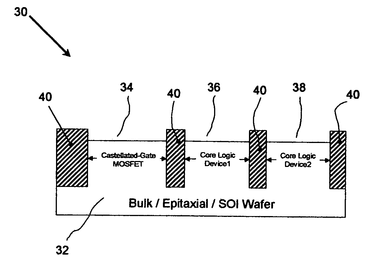
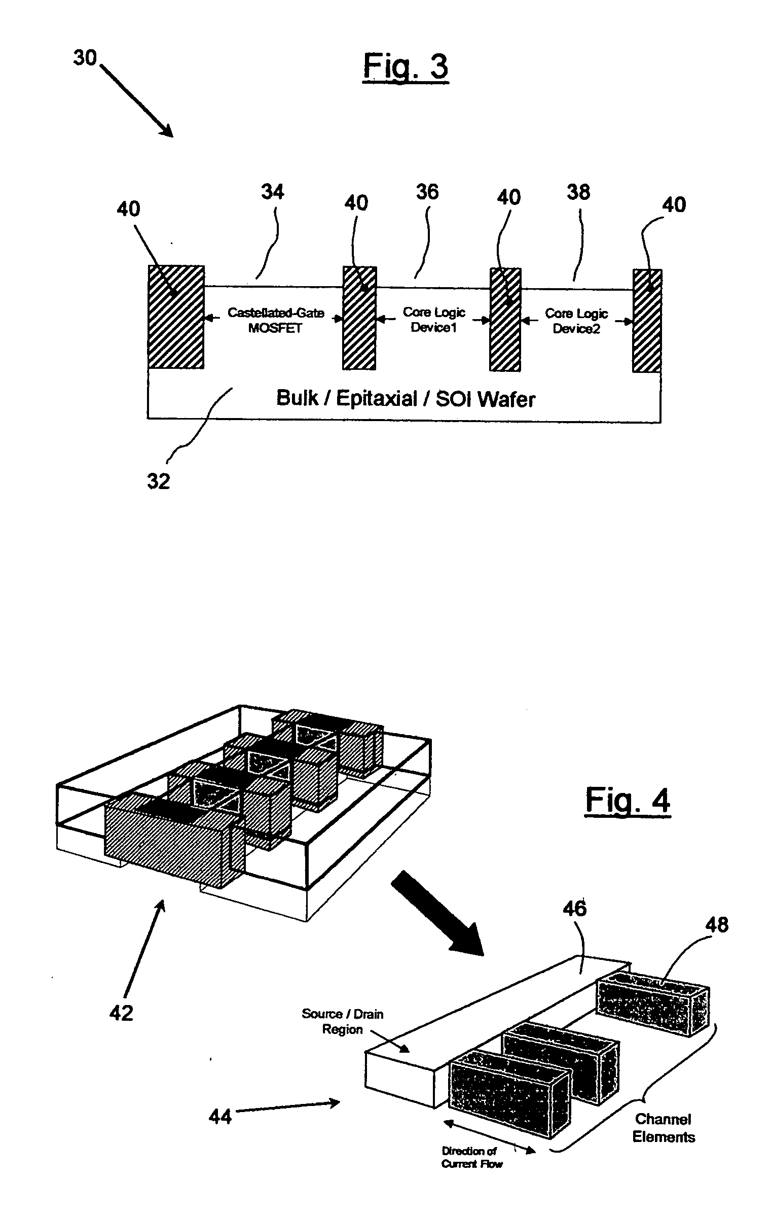
[0095] The combined semiconductor technology platform of the present invention integrates one or more types of logic or memory device with at least one type or polarity of castellated-gate MOSFET device capable of fully depleted operation on a common semiconductor substrate. Referring to FIG. 3., a generic embodiment of a device in accordance with the present invention is illustrated in a crossectional view. The generic combined device embodiment 30 incorporates a castellated gate MOSFET device capable of fully-depleted operation within a region 34, as well as first 36 and second 38 regions designated for first and second types of semiconductor logic devices, respectively. The regions are laterally separated by trench insulator islands 40, and all contained within a common semiconductor substrate 32.

[0096] Within the context of the present invention, a generic castellated-gate MOSFET capable of fully-depleted operation is essentially a vertical dual-gate, or tri-gate “FinFET” device...

first embodiment

[0110] All castellated-gate devices and core logic devices of the combined device 60 all share common contact structures 112 and wiring 114 (as defined by mask layers 90 and 74, respectively, in FIG. 7). In addition, the core logic devices and castellated-gate devices may share regions of same conductivity type, such as a common N-Well 104. The N-Channel and P-Channel castellated-gate devices of this first embodiment share a common silicide blocking film 130, which is typically a deposited and patterned oxide such as TEOS or BPTEOS.

second embodiment

[0111] Referring now to FIG. 8, the of the present invention is illustrated with its photo masking layers using a bulk silicon starting wafer. FIG. 8 illustrates a combined device 61 which incorporates planar CMOS logic consisting of an N-Channel device 64, a P-Channel device 66, as well as two N-Channel castellated-gate MOSFETs 62 having a first threshold voltage (Vt) value and two N-Channel castellated-gate MOSFETs 69 having a second threshold voltage (Vt) value. Each castellated MOSFET of FIG. 8 is shown in a first orientation, as well as a second orientation that is rotated 90 deg from the first. FIG. 8A shows the combined device 61 in a cross-sectional view taken substantially along the line 8A-8A′ of FIG. 8.

[0112] In FIG. 8A, N-Channel castellated-gate devices A1 and A2 having a first threshold voltage value reside within a predefined region A of p-type conductivity in a substrate 100, separated by trench isolation structures 110. Similar to the first embodiment of the present...


PUM


Abstract

A Mixed-Signal Semiconductor Platform Incorporating Castellated-Gate MOSFET device(s) capable of Fully-Depleted operation is disclosed along with a method of making the same. The composite device/technology platform has robust I/O applications and includes a starting semiconductor substrate of a first conductivity type. One or more isolated regions of at least a first conductivity type is separated by trench isolation insulator islands. Within an isolated region designated for castellated-gate MOSFETs there exists a semiconductor body consisting of an upper portion with an upper surface, and a lower portion with a lower surface. Also within the castellated-gate MOSFET region, there exists a source region, a drain region, and a channel-forming region disposed between the source and drain regions, and are all formed within the semiconductor substrate body. The channel-forming region within the isolated castellated-gate MOSFET region is made up of a plurality of thin, spaced, vertically-orientated conductive channel elements that span longitudinally along the device between the source and drain regions. One or more of the trench isolated regions may contain at least one type or polarity of logic and/or memory computing device. Alternately or additionally, one or more type of Logic and/or memory device may be incorporated within vertically displaced regions above the active body region of the semiconductor wafer, embedded within Interlevel Dielectric Layers.

Description


Claims


Application Information

Patent Timeline
Owner IP3 2021 SERIES 600 OF ALLIED SECURITY TRUST I
Why Eureka
Try Eureka