Castellated gate MOSFET device capable of fully-depleted operation

a mosfet device and channel structure technology, applied in the field of field effect transistors, can solve the problems of reducing the power consumption of digital functions

Active Publication Date: 2010-05-11
PALO ALTO NETWORKS INC
View PDF24 Cites 40 Cited by
  • Summary
  • Abstract
  • Description
  • Claims
  • Application Information

AI Technical Summary

Benefits of technology

[0014]Accordingly, it is one object of the present invention to provide an improved, castellated-gate MOSFET device capable of fully depleted operation.
[0017]Still another object of the present invention is to provide a high speed I / O device having enhanced ESD / EOS and reliability characteristics relative to existing VLSI I / O devices for a given wafer area.
[0018]A further object of the present invention is to provide a high speed I / O device that enables circuitry with improved / reduced latch-up susceptibility on non-SOI wafers.
[0019]Yet another object of the present invention is to provide a castellated gate MOSFET device capable of symmetrical operation with respect to the source and drain terminals.
[0020]Another object of the present invention is to provide an area-dense VLSI I / O device with improved thermal conduction properties from the silicon active area (heat dissipation).

Problems solved by technology

While CMOS scaling has enabled the circuit and system designer to pack a tremendous amount of functionality onto a silicon die, it has simultaneously created a number of significant problems as far as the chip's ability to interface with the outside world.
Unfortunately, in such technology evolution, the thick oxide I / O device has become somewhat of a “forgotten stepchild”, as only the thin-oxide core devices can truly take advantage of the shrinking feature sizes that are enabled by state-of-the-art photolithography.
More importantly, as the thick oxide device is a “leftover” from the previous technology node, it typically under-performs the thin-oxide core device in terms of speed / bandwidth (ft).
While this reliability-driven voltage trend results in lower power consumption for digital functions, the effect is not necessarily the same in the analog case.
In fact, it has been shown that in an analog-to-digital converter application with a fixed dynamic range requirement, power consumption can actually increase with decreasing power supply.
More problematic from the standpoint of device reliability and survivability is the significantly harsher EMI (electromagnetic induction) / ESD (electrostatic discharge) environment seen by I / O devices used in mixed-signal communications applications.
However, in a data transmission or communication situation, there is the additional problem of signal reflections due to improperly terminated transmission lines.
In the first two mixed-signal examples, that is system backplane and chip-to-chip, a termination problem could chronically arise due to manufacturing tolerances, or as the result of devices connecting and disconnecting from the bus, or perhaps as a “hot swap” situation.
One of the known causes of latch-up is an ESD event that results in the injection of minority carriers from the clamping device in the protection circuit into either the substrate bulk or the well.
In a harsh I / O environment, transmission line reflections may also trigger the ESD protect device, thus increasing the probability that a latch-up condition can occur.
However, a number of difficulties persist including, in particular, power consumption, cost and scalability.
Bipolar devices consume significantly more power than CMOS devices, which increases package cost and at some point renders them unsuitable as a system solution, in particular for portable devices.
From the standpoint of scaling, bipolar technologies have hit an apparent limit in terms of increasing performance for a given density and power consumption.
The integration of CMOS and bipolar devices (BiCMOS) reduces the power consumption problem but leads to a second difficulty, i.e. cost.
Finally, bipolar devices by nature, like the thick oxide CMOS I / O devices discussed earlier, cannot take full advantage of decreasing feature sizes which result from advances in wafer patterning technology (photolithography).
Clearly, the trends and problems discussed above may soon create a situation where it is no longer desirable to integrate a significant amount of analog functionality into a single-chip mixed-signal system solution, thus eliminating one of the traditional paths to reduce cost and power consumption in electronic systems.
However, these problems still persist.

Method used


Image

  • Castellated gate MOSFET device capable of fully-depleted operation
  • Castellated gate MOSFET device capable of fully-depleted operation
  • Castellated gate MOSFET device capable of fully-depleted operation

Examples


embodiment 72

[0066]Depending on the desired device electrical characteristics, the contacts 66 disposed within interlevel dielectric structure (ILS) 68 to the source and drain structures 24, 26 may be coincident with the upper silicon surface as illustrated in FIG. 3A, or the contacts 67 (as shown in FIG. 4A) may penetrate into the uppermost impurity layer. For example, surface contacts 66 could result in higher series resistance, which would be beneficial in enhancing ESD characteristics. In the particular example of FIGS. 3 and 3A, the contact masks 70 are laid-out in such a way as to be directly in-line with the conductive channels 22. This approach should provide the least device series resistance, thus improving device performance. Furthermore, it should be understood that additional process steps can be added to the overall fabrication sequence to shut-down the bottom gate. Examples are illustrated in the case of a dual-gate embodiment 72 illustrated in FIGS. 4 and 4A, including the additi...

embodiment 78

[0067]FIGS. 5 and 5A illustrate an NMOS device embodiment 78 of the disclosed device invention using a silicon-on-insulator (SOI) starting substrate 80. Note that the device mask layout remains substantially the same as the case of the device 20 with the bulk starting wafer 21 shown in FIGS. 3-3A. Substantially similar to the bulk silicon substrate device 20, the device 78 includes a plurality of thin silicon channel elements 22 that span the distance between a source region 24 and a drain region 26. In the SOI wafer case of the device 78, the device's gate slots 82 can be etched to the same depth as the STI islands 54, 56, that is all the way to the buried oxide 75. However, there are advantages to leaving a common silicon connection 81 in the form of the substrate 21 of FIGS. 3 and 3A at the bottom, thus enabling the use of body contacts which can be employed to eliminate device snapback problems as well as provide a path of higher thermal conductivity with which to dissipate heat...
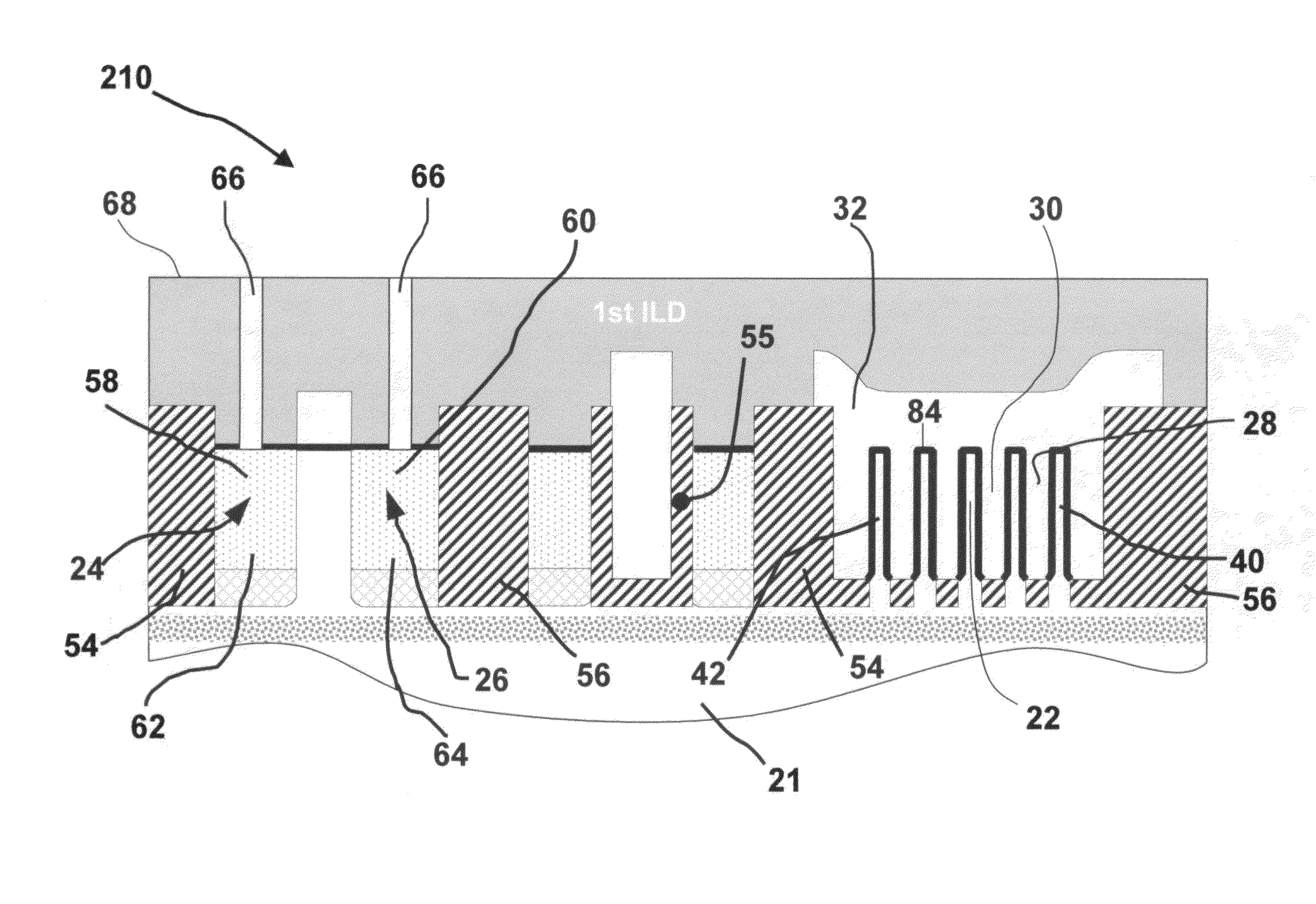
embodiment 216

[0073]FIGS. 8 and 8A illustrate another embodiment 216 of the present invention wherein the spacer dielectric 114, with its associated thick bottom gate 116, (see FIGS. 3-3A and 6-6B) is omitted. Once again, the device mask layout remains substantially the same as the case of the device 20 with the bulk starting wafer 21 as shown in FIGS. 3-3A. However, now the edges of gate mask 51 are coincident with, or preferably slightly overlap, the gate slot mask 49 in the direction of channel length (Ld), as indicated by line 52. In this embodiment, the gate slot trenches 28 are etched to a first predetermined depth that is typically less than the depth of the Shallow Trench Isolation 54, 56.

[0074]As was the case of device 20 (see FIG. 3A), the outer gate slot masks 34, 36 result in the formation of outmost gate conductor elements which simultaneously penetrate into both the silicon and bounding Shallow Trench Isolation (STI) 54, 64 of the device 216. Dual-polarity source and drain regions 2...


PUM


Abstract

A castellated-gate MOSFET I / O device capable of fully depleted operation is disclosed. The device includes a semiconductor substrate region having an upper portion with a top surface and a lower portion with a bottom surface. A source region and a drain region are formed in the semiconductor substrate region, and a channel-forming region is also disposed therein between the source and drain regions. Trench isolation insulator islands, having upper and lower surfaces, surround the source and drain regions as well as the channel-forming region. The channel-forming region includes a plurality of thin, spaced, vertically-orientated conductive channel elements that span longitudinally along the device between the source and drain regions. A gate structure is provided in the form of a plurality of spaced, castellated gate elements interposed between the channel elements, and a top gate member interconnects the gate elements at their upper vertical ends to cover the channel elements. The conductive channel elements are super-self-aligned from the gate structure to the source and drain regions. Finally, a dielectric layer separates the conductive channel elements from the gate structure.

Description

CROSS REFERENCE TO RELATED APPLICATIONS[0001]This application is a continuation-in-part of U.S. patent application Ser. No. 10 / 940,093, filed Sep. 13, 2004, now U.S. Pat. No. 7,211,864, to John J. Seliskar entitled, “An Improved Fully-Depleted Castellated Gate MOSFET Device and Method of Manufacture Thereof”, the contents of which are hereby expressly incorporated herein by reference. In addition, this application relates to co-pending U.S. patent application Ser. No. 11 / 728,111, filed Mar. 23, 2007, to John J. Seliskar entitled, “An Improved Fully-Depleted Castellated Gate MOSFET Device and Method of Manufacture Thereof”, and which is a division of the above-referenced U.S. patent application Ser. No. 10 / 940,093, filed Sep. 13, 2004.BACKGROUND OF THE INVENTION[0002]1. Field of the Invention[0003]The present invention relates generally to field effect transistors (FET's) formed as complimentary metal oxide semiconductor (CMOS) structures and, more particularly, to new and improved M...

Claims


Application Information

Patent Timeline
Patent Type & Authority Patents(United States)
IPC IPC(8): H01L29/94H01L21/336H01L21/84H01L27/12H01L29/423H01L29/786
CPCH01L21/84H01L27/1203H01L29/42384H01L29/78636H01L29/66795H01L29/785H01L29/78612H01L29/66545
Inventor SELISKAR, JOHN J.
Owner PALO ALTO NETWORKS INC
Why Eureka
Try Eureka