PMOS pixel structure with low cross talk for active pixel image sensors

a pixel structure and active pixel technology, applied in the field of image sensors, can solve the problems of high level of pixel-to-pixel cross talk of sensors, inability to reduce cross talk low enough using these techniques for certain applications, and inability to reduce cross talk

Active Publication Date: 2007-05-17
OMNIVISION TECH INC
View PDF23 Cites 128 Cited by
  • Summary
  • Abstract
  • Description
  • Claims
  • Application Information

AI Technical Summary

Benefits of technology

This technology reduces interference between neighboring components in semiconductors made with standard processes. It also minimizes unwanted electrical signals that can affect performance. Overall, this helps improve the quality and efficiency of these devices.

Problems solved by technology

The technical problem addressed in this patent text relates to reducing cross talk between pixels in CMOS image sensors made on p-type silicon substrates without compromising their benefits and advancements achieved through existing mainstream CMOS processes. Existing methods to address cross talk issues involve developing new technology or requiring significant modifications to existing infrastructure, making them less efficient and costly. There is thus a need for a solution that reduces cross talk effectively without affecting the overall performance of CMOS image sensors.

Method used


Image

  • PMOS pixel structure with low cross talk for active pixel image sensors
  • PMOS pixel structure with low cross talk for active pixel image sensors
  • PMOS pixel structure with low cross talk for active pixel image sensors

Examples


Embodiment Construction

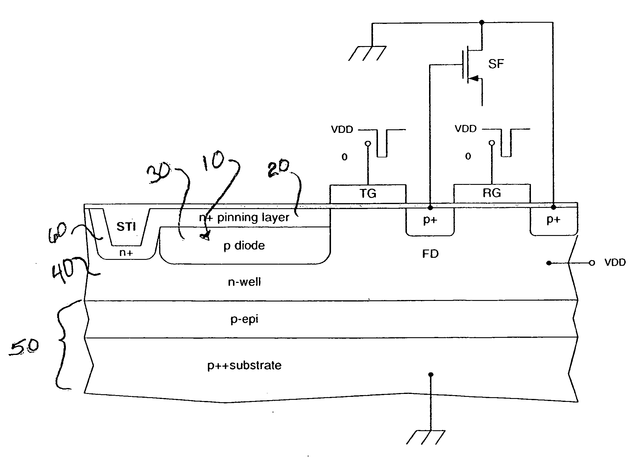
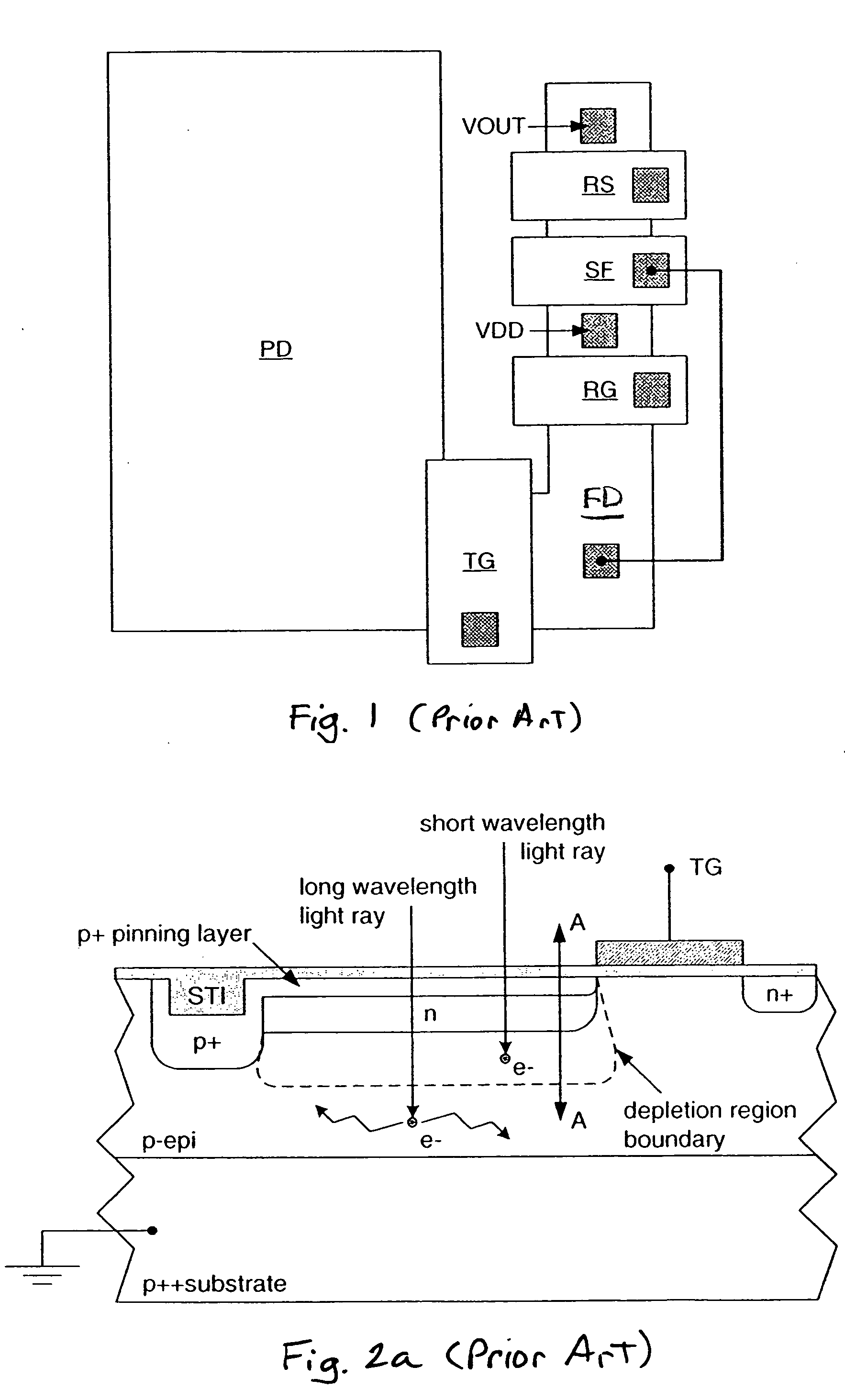
[0021] Historically, charge-coupled device (CCD) -based image sensors have primarily used electrons as the signal-charge carrier to take advantage of their higher mobility to maintain good transfer efficiency at high data rates. To reduce color cross talk and smear, and to provide blooming protection, CCD imagers are also typically built in a well, or vertical-overflow drain (VOD) structure (see for example U.S. Pat. No. 4,527,182). Therefore, building a VOD structure along with the requirement for an n-channel requires that a p-well be formed in an n-type substrate.

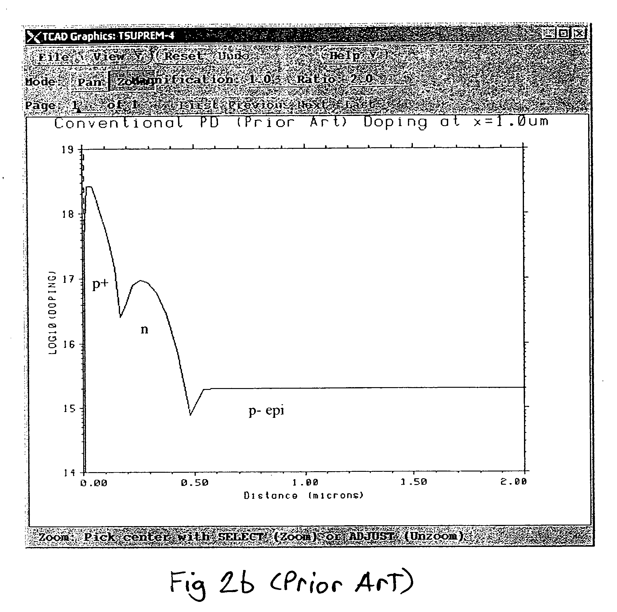
[0022] CMOS-based image sensors have since become more readily available. Current day CMOS image sensors are typically built on either p- or n-type silicon substrates. Those built on p-type substrates using mainstream CMOS processing can contain high levels of circuit integration, but suffer from high levels of color cross talk. Those built using a typical CCD-like process on n-type substrates (S. Inoue et al.,“A 3.25 M...


PUM


Abstract

An image sensor with an image area having a plurality of pixels each having a photodetector of a first conductivity type, the image sensor includes a substrate of the first conductivity type; a first layer of the second conductivity type between the substrate and the photodetectors, spanning the image area and biased at predetermined potential with respect to the substrate for driving excess carriers into the substrate to reduce cross talk; one or more adjacent active electronic components disposed in the first layer within each pixel; and electronic circuitry disposed in the substrate outside of the image area.

Description


Claims


Application Information

Patent Timeline
Owner OMNIVISION TECH INC
Why Eureka
Try Eureka