Display devices and the display panels thereof

a display panel and display technology, applied in semiconductor devices, optics, instruments, etc., can solve the problems of reducing the optical performance of the display panel, affecting the resolution rate and aperture rate, and tft components may have electrical leakage problems, etc., to achieve the effect of reducing the shifted channel of electrons, and reducing space charge area

Active Publication Date: 2018-07-26
WUHAN CHINA STAR OPTOELECTRONICS TECH CO LTD
View PDF2 Cites 2 Cited by
  • Summary
  • Abstract
  • Description
  • Claims
  • Application Information

AI Technical Summary

Benefits of technology

[0026]In view of the above, the display panel includes a first substrate, a second substrate, a liquid crystal layer between the first substrate and the second substrate, a masking layer on the first substrate, a buffering layer arranged on the masking layer and the first substrate, a first semiconductor layer on the buffering layer, and an active layer on the first semiconductor layer and the buffering layer. When the gate driving signals have no bias voltage, the active first semiconductor la...

Problems solved by technology

With respect to liquid crystal panel, thin film transistor (TFT) components may have the electrical leakage issue.
The unstable grayscale value may downgrade the opt...

Method used


Image

  • Display devices and the display panels thereof
  • Display devices and the display panels thereof
  • Display devices and the display panels thereof

Examples


Embodiment Construction

[0031]Embodiments of the invention will now be described more fully hereinafter with reference to the accompanying drawings, in which embodiments of the invention are shown.

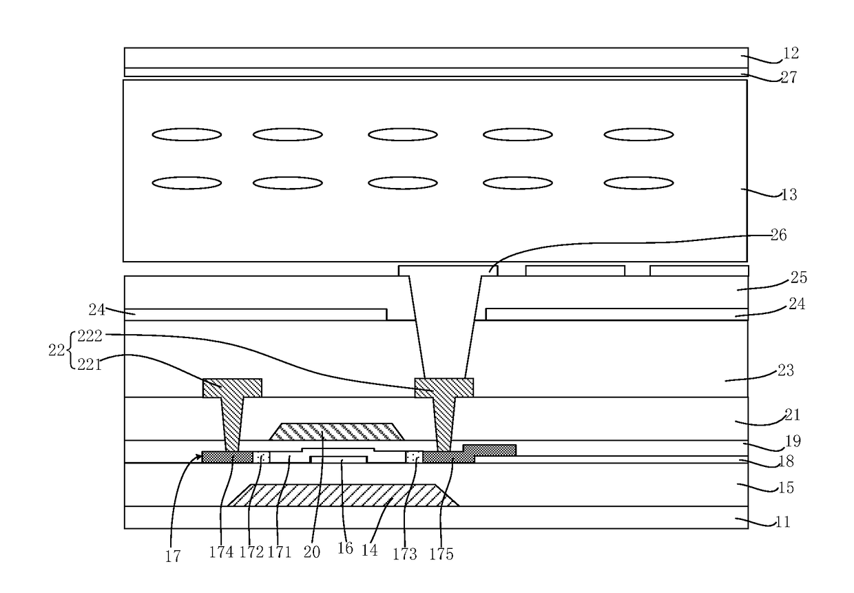
[0032]FIG. 1 is a schematic view of the display panel in accordance with one embodiment. The display panel includes a first substrate 11, a second substrate 12, a liquid crystal layer 13 between the first substrate 11 and the second substrate 12, a masking layer 14 on the first substrate 11, a buffering layer 15 arranged on the masking layer 14 and the first substrate 11, a first semiconductor layer 16 on the buffering layer 15, and an active layer 17 on the first semiconductor layer 16 and the buffering layer 15.

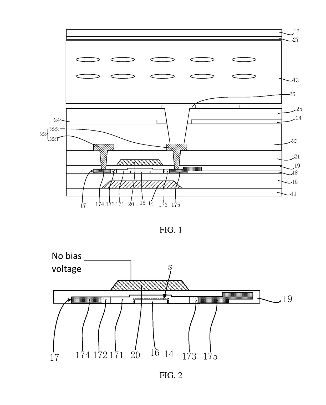
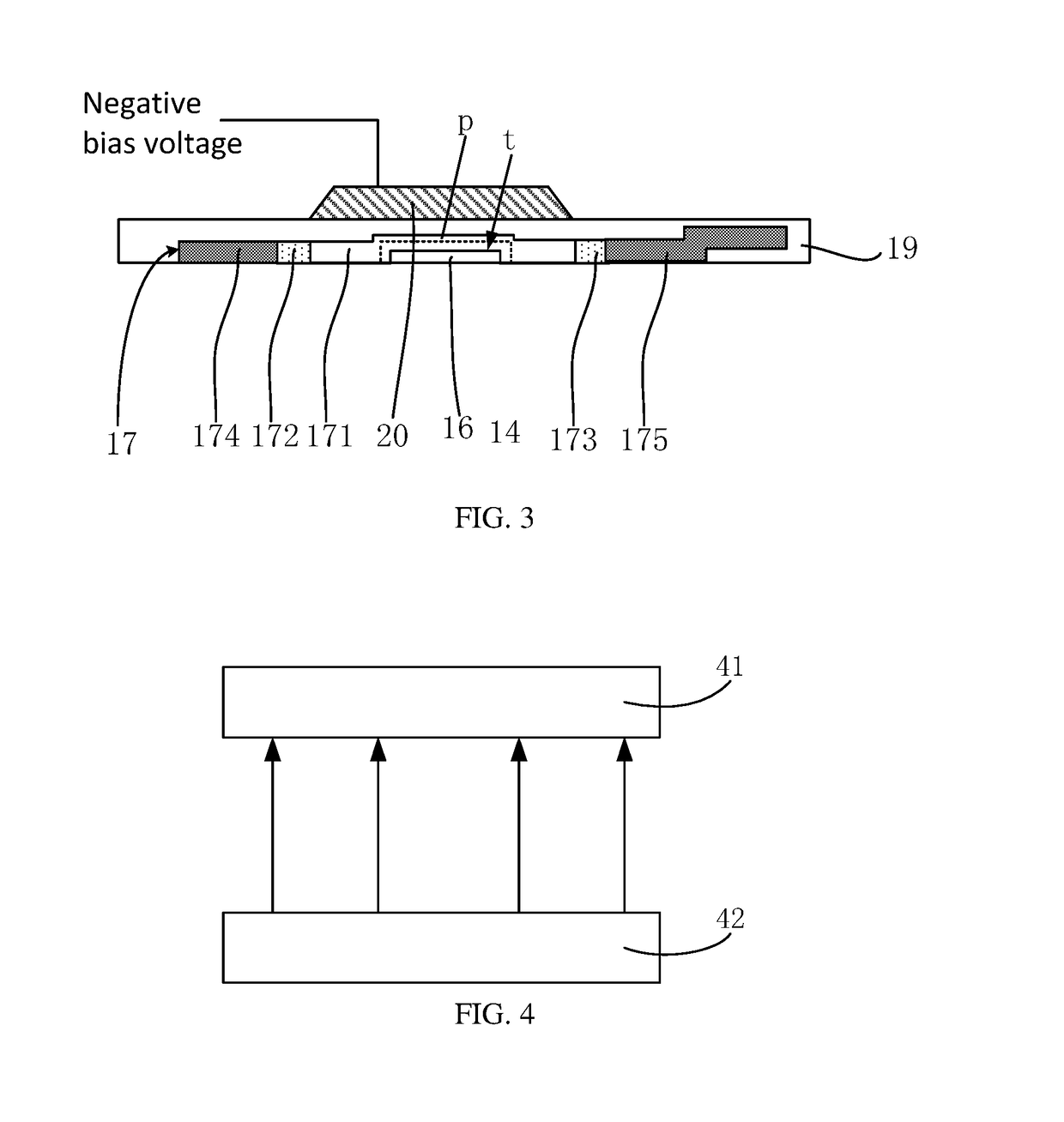
[0033]As the first semiconductor layer 16 is formed below the active layer 17, when the gate driving signals have no bias voltage, the active first semiconductor layer 16 and the active layer 17 form a PN junction and a very thin space charge area is formed in the PN junction. When the gate driving signa...


PUM


Abstract

The present disclosure relates to a display panel including a first substrate, a second substrate, a liquid crystal layer between the first substrate and the second substrate, a masking layer on the first substrate, a buffering layer arranged on the masking layer and the first substrate, a first semiconductor layer on the buffering layer, and an active layer on the first semiconductor layer and the buffering layer. The present disclosure also relates to a display device. With such configuration, the leakage current of the TFTs may be reduced, which also reduces the cross-talk and the flicker of the liquid crystal panel.

Description

BACKGROUND OF THE INVENTION1. Field of the Invention[0001]The present disclosure relates to display technology, and more particularly to a display device and the display panel thereof.2. Discussion of the Related Art[0002]LCDs typically are characterized by attributes including thin, power-saving, and low radiation, and thus are very popular display devices. Currently, cellular phones often adopt Fringe Field Switching (FFS) display mode for the reason that the viewing angle is wider and may not be easily affected by the thickness of the liquid crystal cell.[0003]With respect to liquid crystal panel, thin film transistor (TFT) components may have the electrical leakage issue. A greater storage capacitance (Cst) has to be configured to prevent the grayscale value of the pixels from TFT electrical leakage within one frame. The unstable grayscale value may downgrade the optical performance of the display panel, such as cross-talk and flicker. However, the storage capacitance (Cst) may ...

Claims


Application Information

Patent Timeline
IPC IPC(8): G02F1/1368H01L29/786G02F1/1362
CPCG02F1/1368H01L29/78624G02F1/136209H01L29/78633H01L29/7869H01L29/78609H01L29/78696G02F2001/13685G02F2001/134372G02F1/134363G02F1/136227H01L27/1225G02F1/136213G02F1/13685G02F1/134372G02F1/1362
Inventor MA, LIANGZHAO, MANG
Owner WUHAN CHINA STAR OPTOELECTRONICS TECH CO LTD
Why Eureka
Try Eureka