

Method of forming resistor of flash memory device
a technology of flash memory and resistor, which is applied in the direction of resistors, semiconductor devices, electrical devices, etc., can solve the problems of large area required, complicated drawing rules, and difficulty in ensuring process margins
- Summary
- Abstract
- Description
- Claims
- Application Information
AI Technical Summary
Problems solved by technology
Method used
Image

Examples
Embodiment Construction
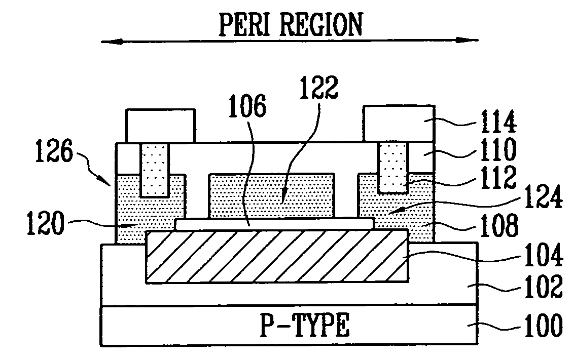
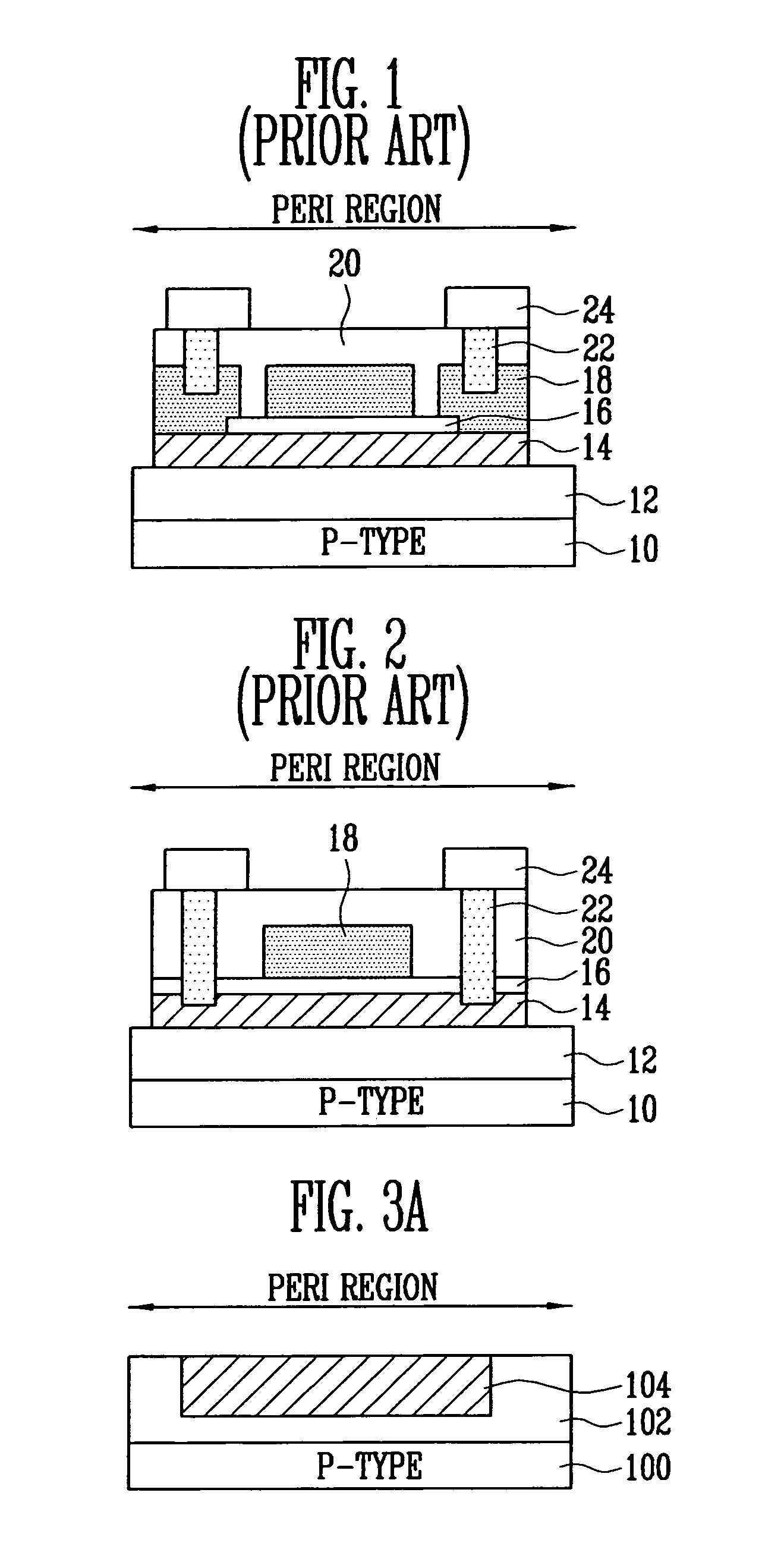
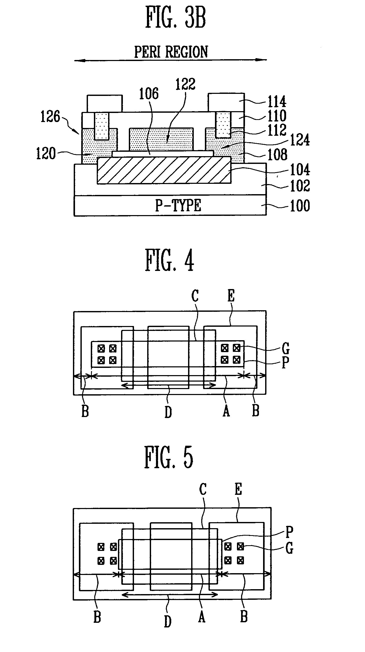
[0025]FIGS. 3A and 3B are cross-sectional views illustrating a method of forming a resistor of a flash memory device according to one embodiment of the present invention. FIGS. 3A and 3B illustrate a method of forming a resistor in a predetermined region of a peri region while forming a gate in which a floating gate and a control gate are laminated in a cell region.
[0026]Referring to FIG. 3A, an isolation structure 102 is formed on a P-type semiconductor substrate 100. A Polysilicon Resistor Mask (PRM) pattern (not shown) is formed on the isolation structure 102. The isolation structure 102 is etched using the PRM pattern (not shown), forming a trench.
[0027]A first polysilicon layer (not shown) is formed on the entire structure so that the trench is filled. The first polysilicon layer is polished until a top surface of the isolation structure 102 is exposed, thus forming a first polysilicon structure 104 within the isolation structure 102. The polishing process may be performed usin...
PUM
 Abstract
Description
Claims
Application Information