

Insulator film, capacitor element, dram and semiconductor device
a capacitor element and semiconductor technology, applied in the direction of fixed capacitors, fixed capacitor details, thin/thick film capacitors, etc., can solve the problems of inability to realize the performance of the capacitor, increase the surface roughness, and deterioration of the capacitance properties, etc., to suppress the surface roughness, and reduce the cost of production
- Summary
- Abstract
- Description
- Claims
- Application Information
AI Technical Summary
Benefits of technology
Problems solved by technology
Method used
Image

Examples
experimental example 1
[0075]A specimen composed of the laminar structure shown in FIG. 2 was manufactured as described below, and the experiments described below were conducted.
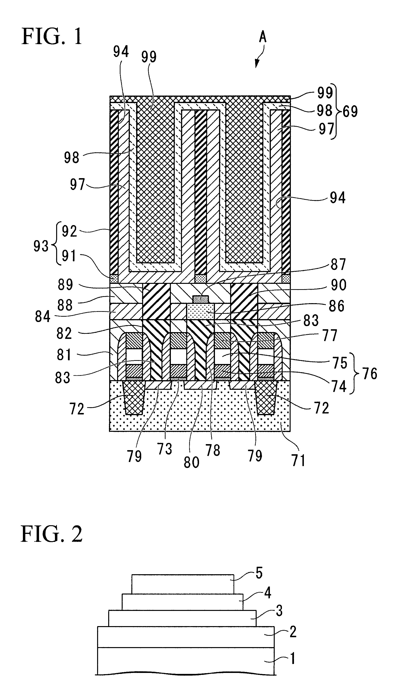
[0076]In FIG. 2, code number 1 indicates an Si substrate, code number 2 a thermal oxide film composed of SiO2, code number 3 a lower electrode composed of Pt film, code number 4 an insulator film, and code number 5 an upper electrode composed of Pt (platinum) film.
[0077]In order to obtain the laminar structure shown in FIG. 2, first, the Si substrate 1 is prepared on the top face of which is formed the thermal oxide film 2 composed of SiO2 used for interdiffusion prevention. Next, a lower electrode 3 is formed on top of the thermal oxide film 2 of the Si substrate 1 by forming Pt film with a film thickness of 100 nm by the sputtering method.
[0078]Subsequently, the insulator film 4 composed of titanium dioxide was formed on top of the lower electrode 3 by the sputtering method. Formation of the insulator film 4 was conducted by arr...
experimental example 2
[0098]Specimens with the laminar structure shown in FIG. 2 were manufactured as described below and subjected to the experiments described below in the same manner as Experimental Example 1, except that the insulator film 4 composing the laminar structure shown in FIG. 2 was an insulator film composed of HfO2 or an insulator film composed of titanium dioxide to which Hf was added.
[0099]That is, as in Experimental Example 1, an insulator film 4 composed of HfO2 was formed on top of the lower electrode 3 by the sputtering method, on top of the Si substrate 1 formed up to the lower electrode 3. Formation of the insulator film 4 was conducted by arranging a HfO2 target inside the chamber, and by supplying 50 W of RF (high-frequency) power to the HfO2 target and causing discharge while rotating the Si substrate 1 which was arranged at a position opposite the target, with the temperature of the Si substrate 1 formed up to the lower electrode 3 set to 300° C., and the chamber pressure set ...
experimental example 3
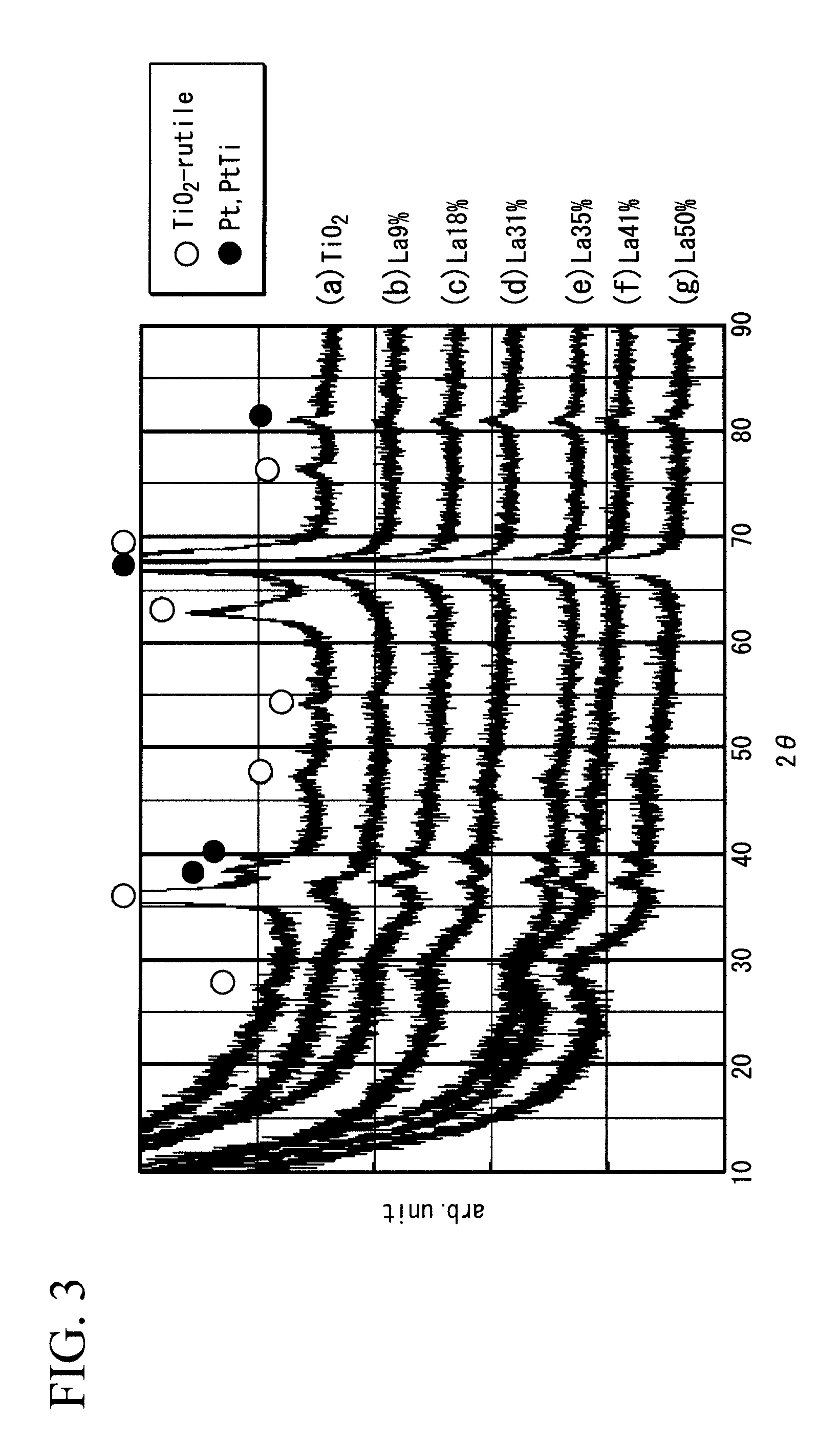
[0110]Specimens with the laminar structure shown in FIG. 2 having insulator films 4 composed of titanium dioxide film with differing Hf additive content (Hf / (Hf+Ti)) ranging from 8% to 78% were manufactured in the same manner as Experimental Example 2, except that the post-annealing temperature was set to 500° C. or 600° C., and the experiments described below were conducted.
[0111]That is, laminar structures were formed having insulator films 4 composed of titanium dioxide film whose Hf additive amount was 8%, 20%, 27%, 37%, 43%, 53% and 78%. With respect to each of these, the relative dielectric constant and breakdown voltage (electric field when leak current density reaches 1E-8A / cm2) were measured. The results are shown in FIG. 7.
[0112]FIG. 7A is a graph that shows the relation of the Hf additive amount (Hf / (Hf+Ti)) in titanium dioxide film and the relative dielectric constant. As shown in FIG. 7A, it is clear that there is little difference between the case where the post-anneal...
PUM
| Property | Measurement | Unit |
|---|---|---|
| relative dielectric constant | aaaaa | aaaaa |
| relative dielectric constants | aaaaa | aaaaa |
| relative dielectric constant | aaaaa | aaaaa |
Abstract
Description
Claims
Application Information