
Microneedle devices and methods of manufacture and use thereof
Patent Information
- Authority / Receiving Office
- US · United States
- Current Assignee / Owner
- Publication Date
- 2009-05-21
- Estimated Expiration
- Not applicable · inactive patent
Smart Images
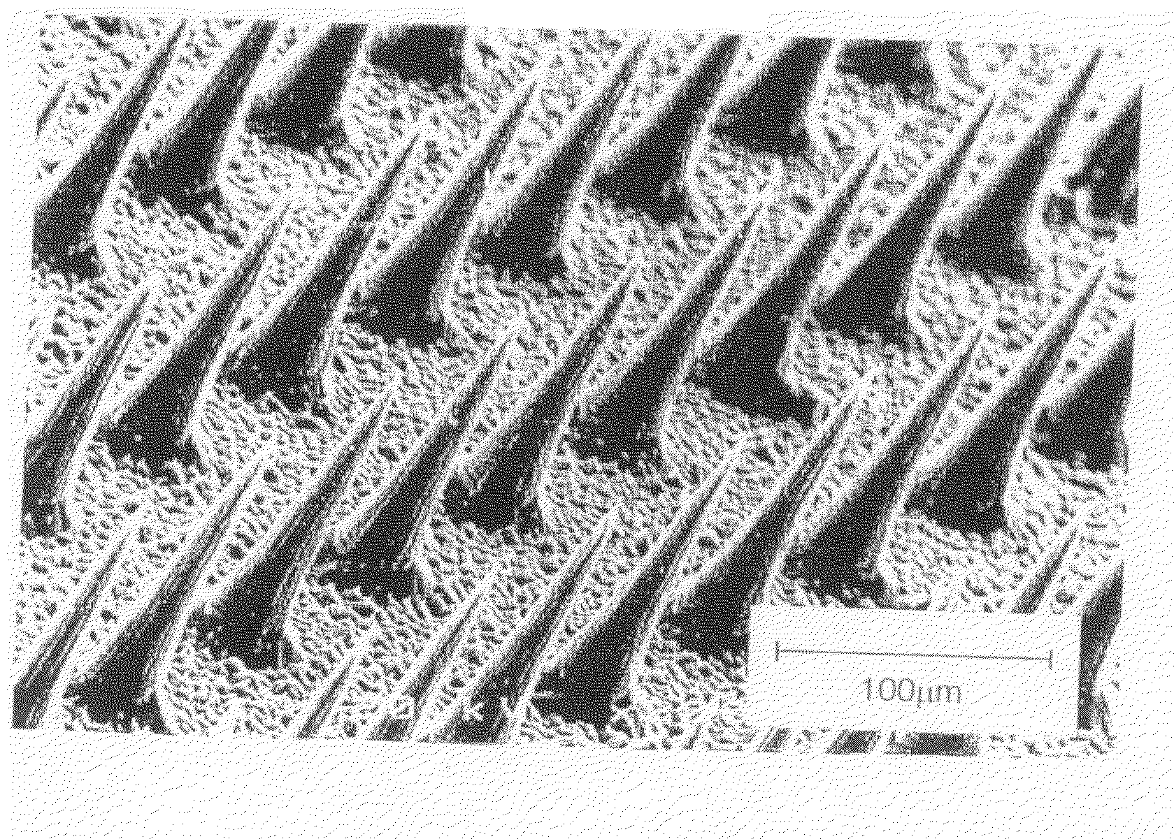
Figure 1 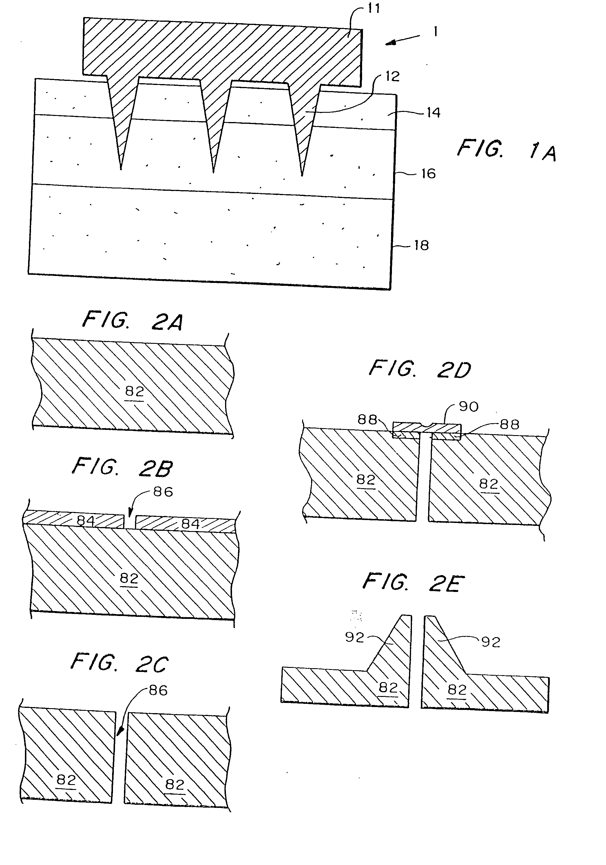
Figure 2 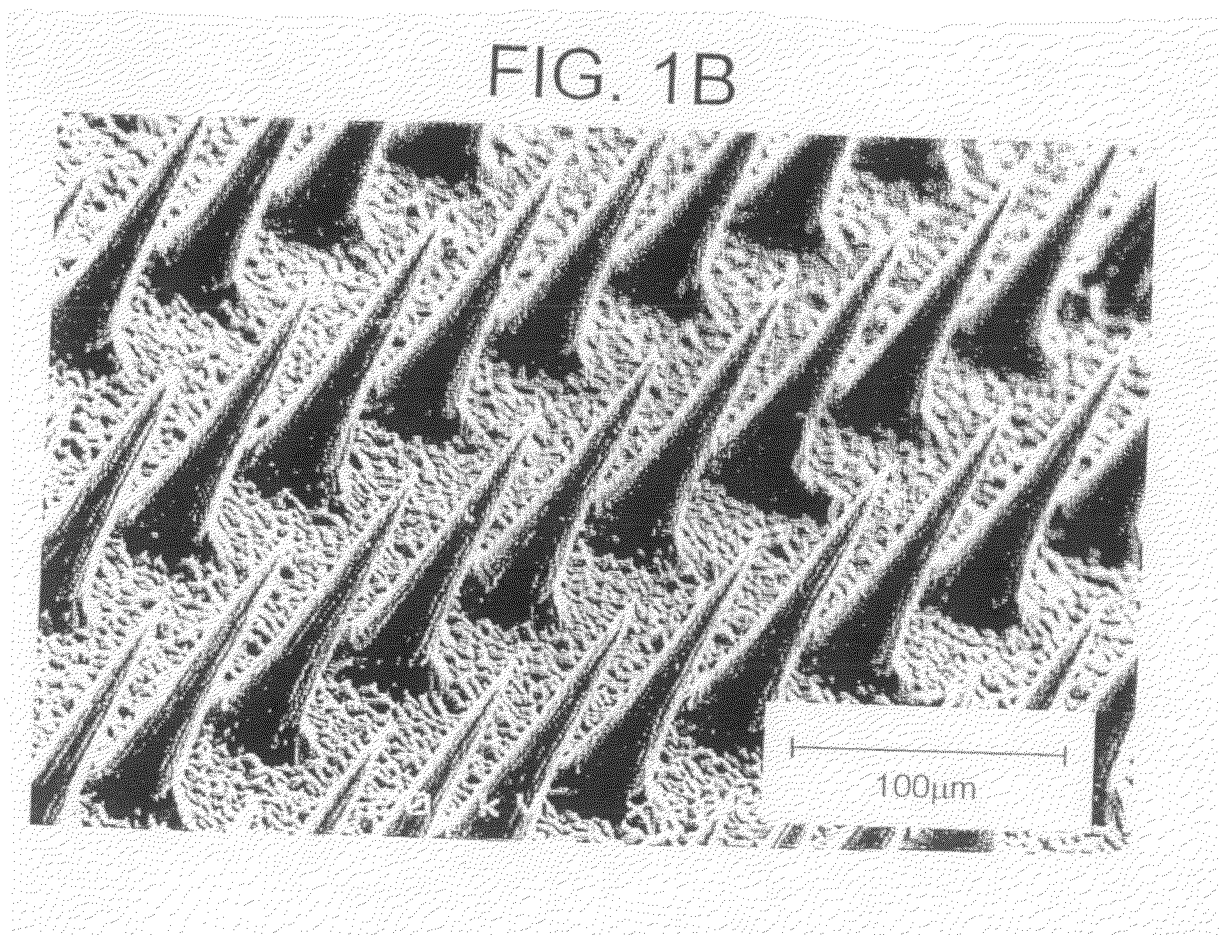
Figure 3
Abstract
Description
CROSS-REFERENCE TO RELATED APPLICATIONS
[0001] This is a continuation-in-part of U.S. Ser. No. 09 / 095,221, filed Jun. 10, 1998.STATEMENT REGARDING FEDERALLY SPONSORED RESEARCH
[0002] The government has certain rights in this invention by virtue of Grant Number BES-9813321 awarded by the U.S. National Science Foundation to Mark R. Prausnitz, and support from the Defense Advanced Research Projects Agency (DARPA) to Mark G. Allen.BACKGROUND OF THE INVENTION
[0003] This invention is generally in the field of devices for the transport of therapeutic or biological molecules across tissue barriers, such as for drug delivery.
[0004] Numerous drugs and therapeutic agents have been developed in the battle against disease and illness. However, a frequent limitation of these drugs is their delivery: how to transport drugs across biological barriers in the body (e.g., the skin, the oral mucosa, the blood-brain barrier), which normally do not transport drugs at rates that are therapeutically useful or op...
Examples
example 1
Fabrication of Solid Silicon Microneedles
[0138]A chromium masking material was deposited onto silicon wafers and patterned into dots having a diameter approximately equal to the base of the desired microneedles. The wafers were then loaded into a reactive ion etcher and subjected to a carefully controlled plasma based on fluorine / oxygen chemistries to etch very deep, high aspect ratio valleys into the silicon. Those regions protected by the metal mask remain and form the microneedles.
[0139]-oriented, prime grade, 450-550 μm thick, 10-15 Ω-cm silicon wafers (Nova Electronic Materials Inc., Richardson, Tex.) were used as the starting material. The wafers were cleaned in a solution of 5 parts by volume deionized water, 1 part 30% hydrogen peroxide, and 1 part 30% ammonium hydroxide (J. T. Baker, Phillipsburg, N.J.) at approximately 80° C. for 15 minutes, and then dried in an oven (Blue M Electric, Watertown, Wis.) at 150° C. for 10 minutes. Approximately 1000 Å of chromium (Mat-Vac Tec...
example 2
Transdermal Transport Using Solid Microneedles
[0142]To determine if microfabricated microneedles could be used to enhance transdermal drug delivery, arrays of microneedles were made using a deep plasma etching technique. Their ability to penetrate human skin without breaking was tested and the resulting changes in transdermal transport were measured.
[0143]Arrays of microneedles were fabricated having extremely sharp tips (radius of curvature less than 1 μm) which facilitate easy piercing into the skin, and are approximately 150 μm long. Because the skin surface is not flat due to dermatoglyphics and hair, the full length of these microneedles will not penetrate the skin. All experiments were performed at room temperature (23±2° C.).
[0144]The ability of the microneedles to pierce skin without breaking was then tested. Insertion of the arrays into skin required only gentle pushing. Inspection by light and electron microscopy showed that more than 95% of microneedles within an array pi...
example 3
Fabrication of Silicon Microtubes
[0148]Three-dimensional arrays of microtubes were fabricated from silicon, using deep reactive ion etching combined with a modified black silicon process in a conventional reactive ion etcher. The fabrication process is illustrated in FIGS. 5a-d. First, arrays of 40 μm diameter circular holes 32 were patterned through photoresist 34 into a 1 μm thick SiO2 layer 36 on a two inch silicon wafer 38 (FIG. 5a). The wafer 38 was then etched using deep reactive ion etching (DRIE) (Laermer, et al., “Bosch Deep Silicon Etching: Improving Uniformity and Etch Rate for Advanced MEMS Applications,”Micro Electro Mechanical Systems, Orlando, Fla., USA (Jan. 17-21, 1999)) in an inductively coupled plasma (ICP) reactor to etch deep vertical holes 40. The deep silicon etch was stopped after the holes 40 are approximately 200 μm deep into the silicon substrate 38 (FIG. 5b) and the photoresist 34 was removed. A second photolithography step patterned the remaining SiO2 la...