

Semiconductor device and method of fabricating the same
a semiconductor memory device and semiconductor technology, applied in the direction of semiconductor memory devices, electrical devices, transistors, etc., can solve the problems of reducing the size of the semiconductor memory device, affecting the operation of the device, so as to prevent the occurrence of dishing or the like, increase the chip area, and the effect of increasing the chip area
- Summary
- Abstract
- Description
- Claims
- Application Information
AI Technical Summary
Benefits of technology
Problems solved by technology
Method used
Image

Examples
Embodiment Construction
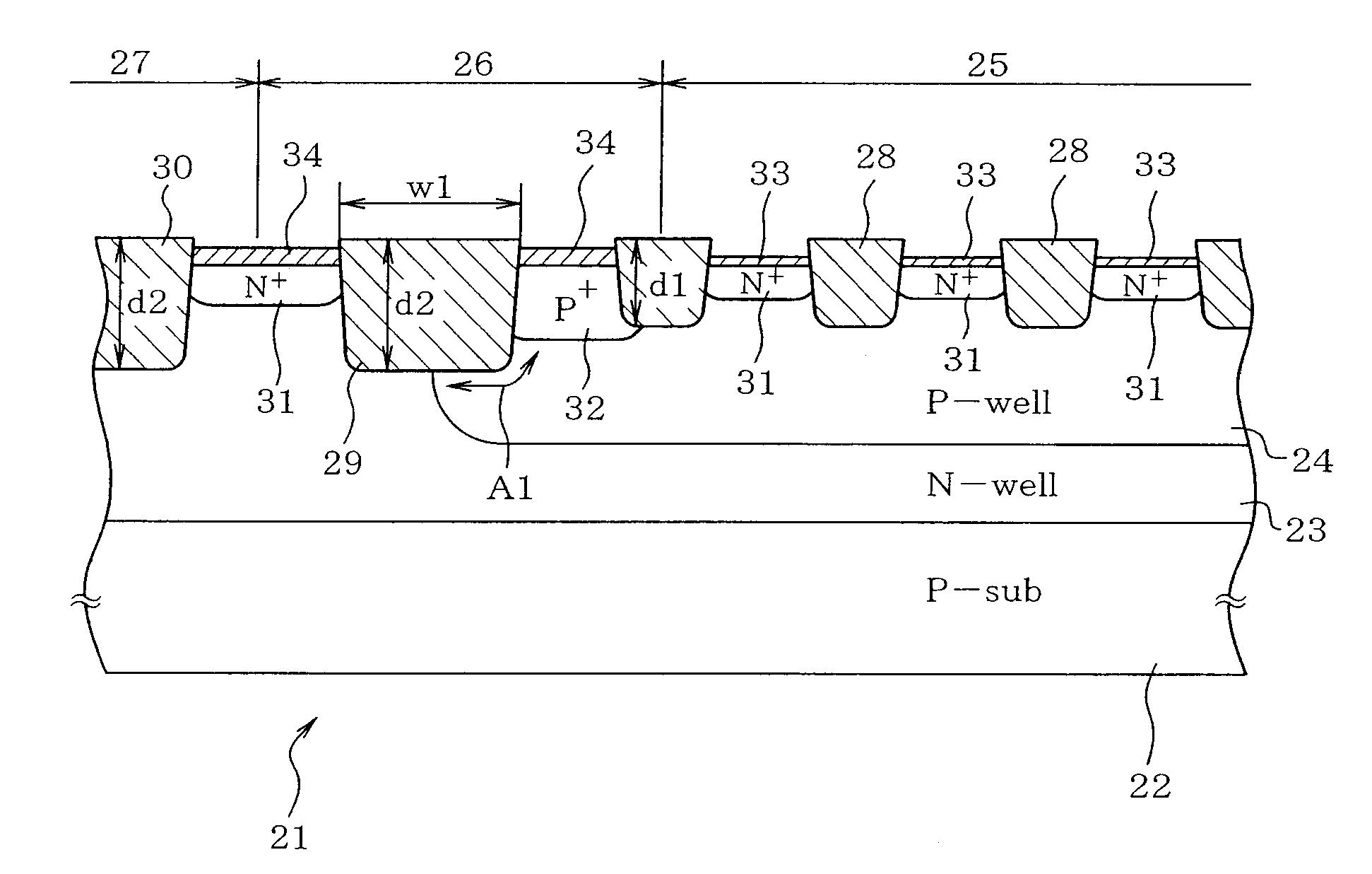
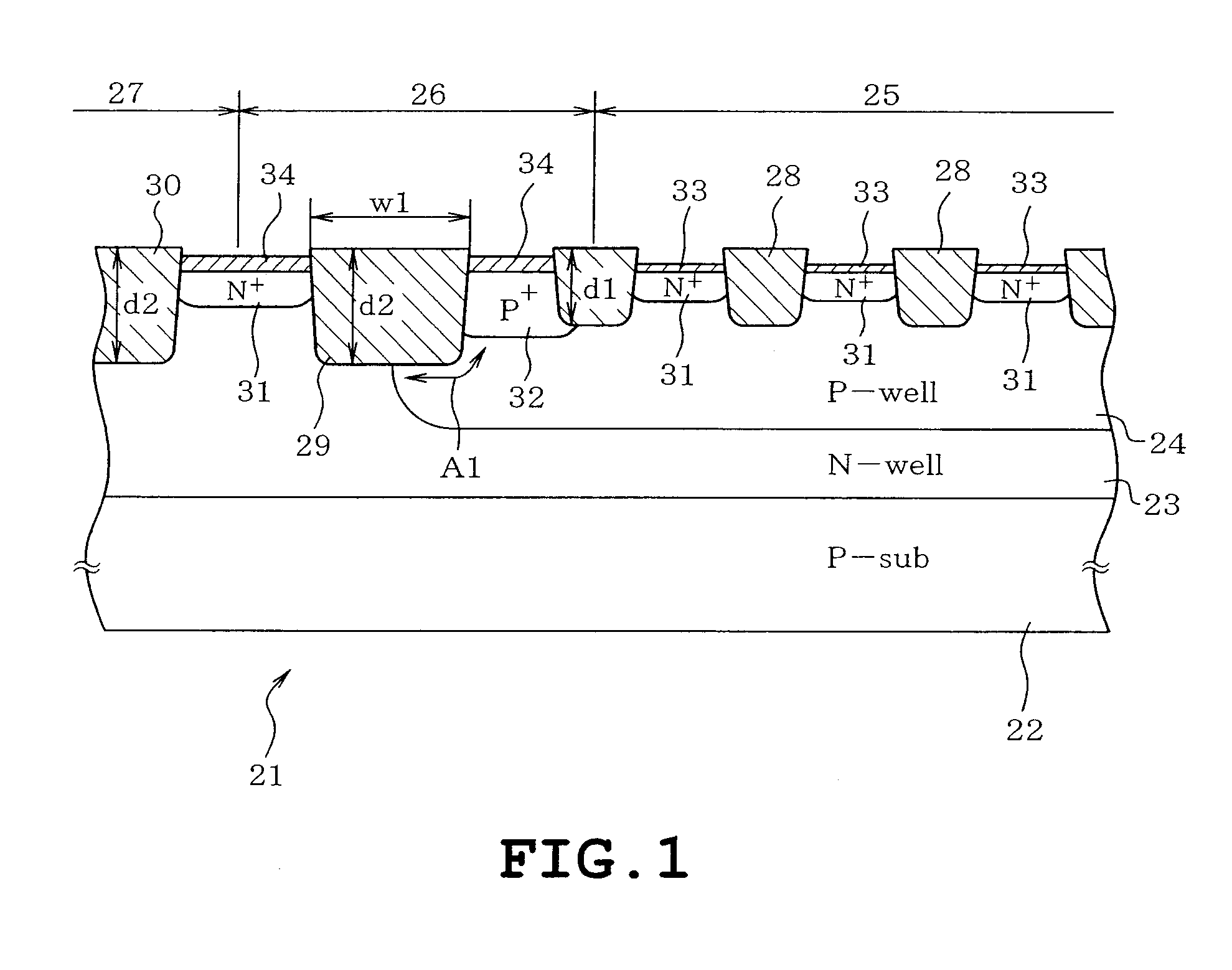
[0034]One embodiment of the present invention will be described with reference to the accompanying drawings. In the following embodiment, the invention is applied to a semiconductor device represented by a flash memory (non-volatile memory) in which elements are isolated by a self-aligned STI method in which an STI doping process is carried out after formation of gate dielectric films.
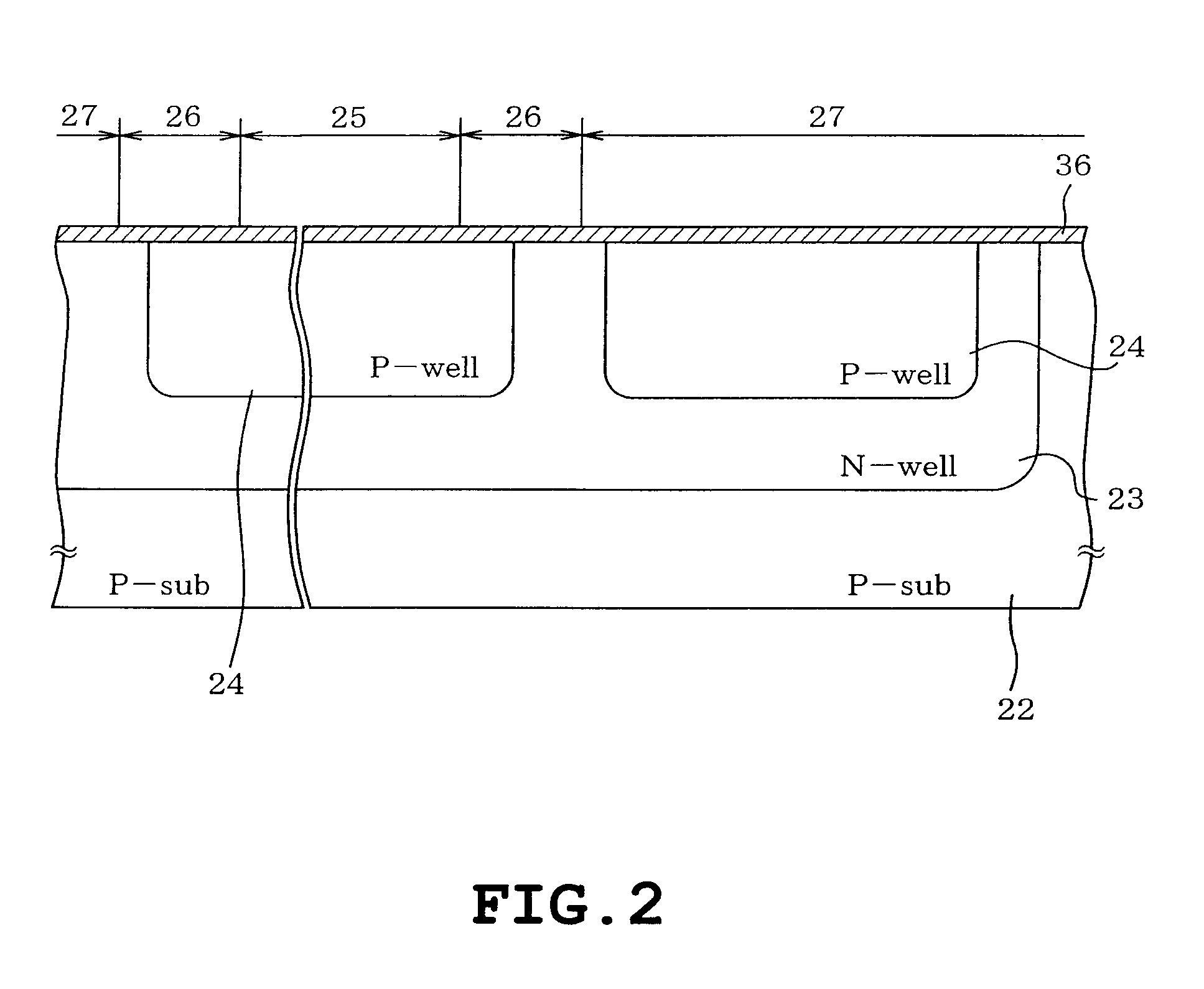
[0035]Referring to FIG. 1, the structure of a non-volatile memory 21 is shown as a semiconductor device fabricated by the fabricating method as will be described later. A p-type (a first conduction type) silicon substrate (P-sub) 22 serving as a semiconductor substrate is formed with an N-well 23 serving as a first well. A P-well 24 serving as a second well is formed in the N-well 23. A memory-cell forming region 25 is formed in the P-well 24. A boundary region 26 is formed in a peripheral portion of the P-well 24. A peripheral circuit 27 is formed outside the P-well 24. The peripheral circuit region 2...
PUM
 Abstract
Description
Claims
Application Information