White organic light emitting device and method for manufacturing the same

a light-emitting device and organic technology, applied in the direction of thermoelectric devices, electroluminescent light sources, electric lighting sources, etc., can solve the problems of poor color reproduction ratio and color shift, and achieve the effect of enhancing the light-emitting efficiency of the hole transport layer and preventing color shi

Active Publication Date: 2010-06-03
LG DISPLAY CO LTD
View PDF1 Cites 59 Cited by
  • Summary
  • Abstract
  • Description
  • Claims
  • Application Information

AI Technical Summary

Benefits of technology

[0017]An object of the present invention is to provide a white organic light emitting device and a method for manufacturing the same, in which a hole transport layer is made to have an energy level higher than an energy level of an excited state of a phosphorescent light emitting layer adjacent thereto for enhancing light emitting efficiency of the hole transport layer without an additional exciton blocking layer, and a dopant content in the phosphorescent light emitting layer is adjusted for preventing color shift from taking place.

Problems solved by technology

However, since the shadow mask sags due to gravity if the shadow mask is large, is difficult to use many times, and has defects occurred in organic light emitting layer formation, alternatives have been required.
However, there is limitations of composition of the dopants contained in the light emitting layers due to the properties of the dopants themselves, and, since mix of the light emitting layers is focused on production of a white light, to have a white wavelength characteristic that has a uniform peak value at a white wavelength region other than red, green, and blue wavelength regions, a color reproduction ratio becomes poor when the color filter is included to the white organic light emitting device.
Moreover, since materials of the dopants are different from one another, if the white organic light emitting device is used continuously, color shift takes place.

Method used


Image

  • White organic light emitting device and method for manufacturing the same
  • White organic light emitting device and method for manufacturing the same
  • White organic light emitting device and method for manufacturing the same

Examples


Embodiment Construction

[0038]Reference will now be made in detail to the specific embodiments of the present invention, examples of which are illustrated in the accompanying drawings. Wherever possible, the same reference numbers will be used throughout the drawings to refer to the same or like parts.

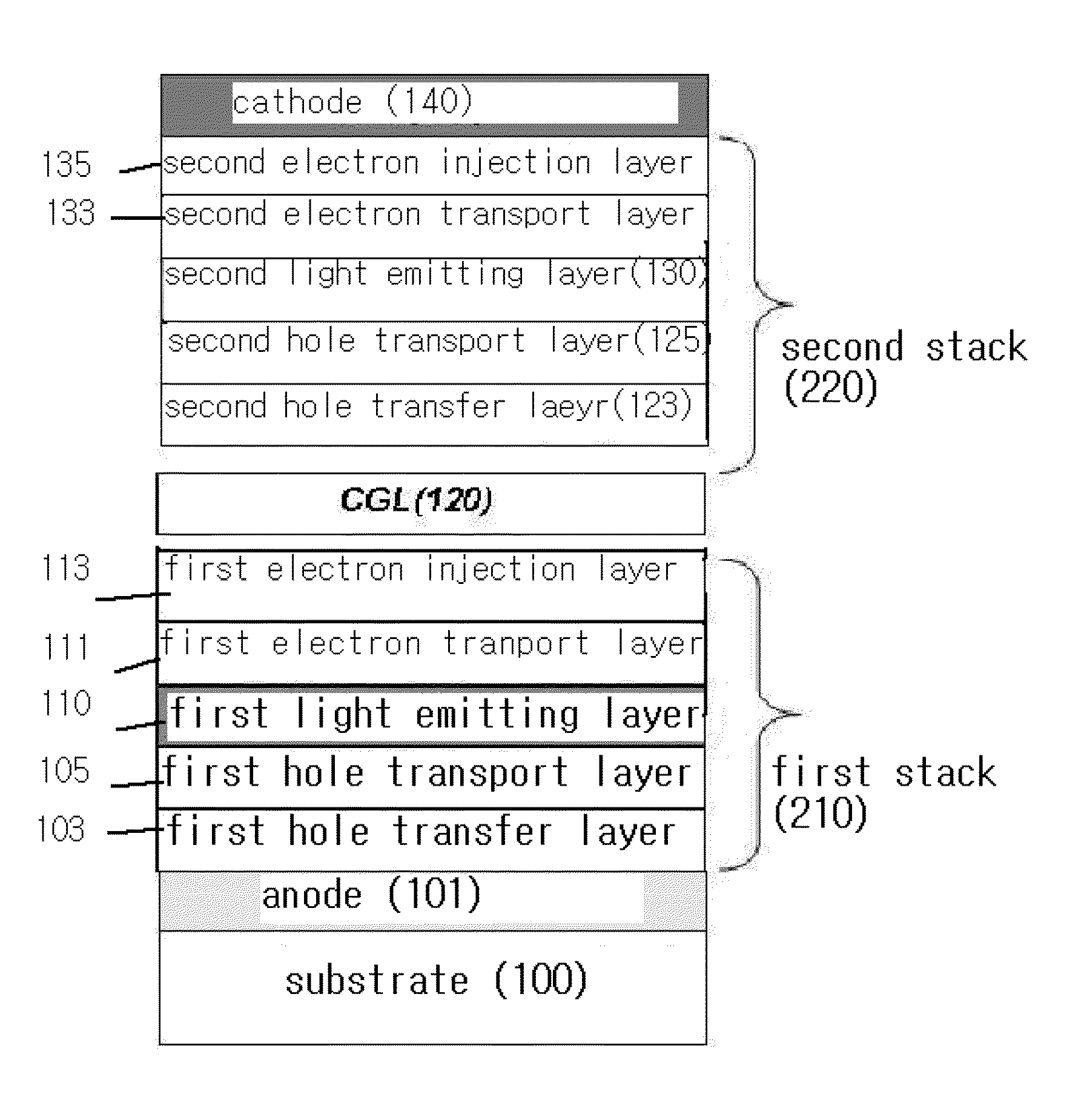
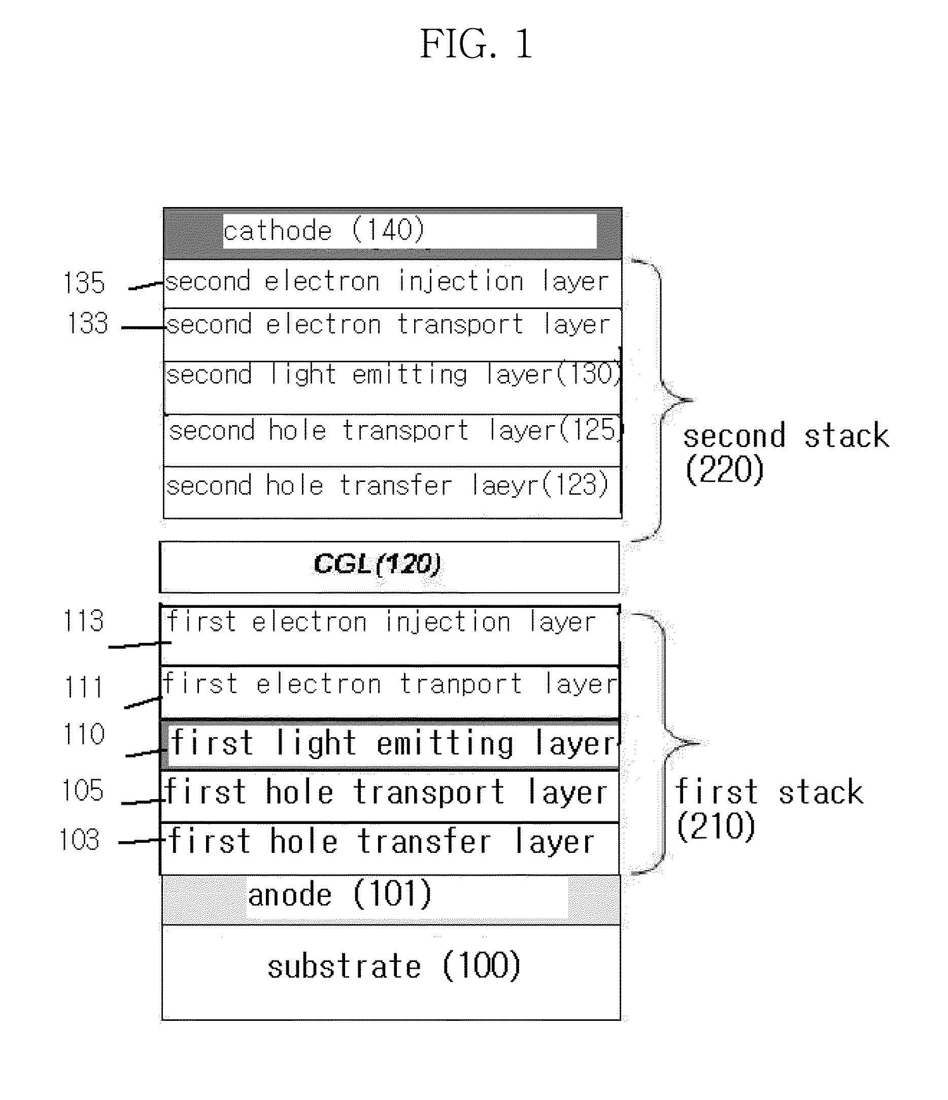
[0039]FIG. 1 illustrates a section of a white organic light emitting device in accordance with a preferred embodiment of the present invention, schematically.

[0040]Referring to FIG. 1, the white organic light emitting device includes opposite anode 101 and cathode 140 on a substrate 100, a first stack 210 between the anode 101 and the cathode 140, a charge generation layer 120 and a second stack 220.

[0041]The anode 101 is formed of a transport electrode, such as ITO (Indium Tin Oxide), and the cathode 140 is formed of a reflective metal, such as Al. Owing to respective light emission from the first and second stacks 210 and 220 arranged as above, an image is forwarded to a lower side of the drawing.
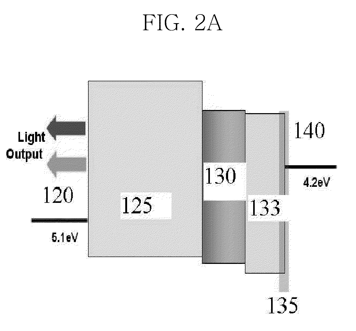
[0042]The ...


PUM


Abstract

The present invention relates to a white organic light emitting device and a method for manufacturing the same, in which a hole transport layer is made to have an energy level higher than an energy level of an excited state of a phosphorescent light emitting layer adjacent thereto for enhancing light emitting efficiency of the hole transport layer without an additional exciton blocking layer, and a dopant content in the phosphorescent light emitting layer is adjusted for preventing color shift from taking place.
The white organic light emitting device includes an anode and a cathode placed on a substrate opposite to each other, a charge generation layer formed between the anode and the cathode, a first stack of a first hole transport layer, a first light emitting layer for emitting a blue light, and a first electron transport layer between the anode and the charge generation layer, and a second stack of a second hole transport layer, a second light emitting layer having a host doped with phosphorescence red and green together, and a second electron transport layer between the charge generation layer and the cathode, wherein the second hole transport layer has an energy level set higher than a triplet excited state energy level of the second light emitting layer.

Description

CROSS REFERENCE TO RELATED APPLICATION[0001]This application claims the benefit of the Patent Korean Application No. 10-2008-0120626, filed on Dec. 1, 2008, which is hereby incorporated by reference as if fully set forth herein.BACKGROUND OF THE DISCLOSURE[0002]1. Field of the Disclosure[0003]The present invention relates to organic light emitting devices, and, more particularly, to a white organic light emitting device and a method for manufacturing the same, in which a hole transport layer is made to have an energy level higher than an energy level of an excited state of a phosphorescent light emitting layer adjacent thereto for enhancing light emitting efficiency of the hole transport layer without an additional exciton blocking layer, and a dopant content in the phosphorescent light emitting layer is adjusted for preventing color shift from taking place.[0004]2. Discussion of the Related Art[0005]Currently, as an information oriented age has come fully, a field of display which ...

Claims


Application Information

Patent Timeline
Patent Type & Authority Applications(United States)
IPC IPC(8): H01L33/00
CPCH01L27/3209H01L51/006H01L51/5278H01L51/5048H01L51/5016H10K59/32H10K85/633H10K50/131H10K50/11H10K2101/10H10K50/14H10K50/19H05B33/20H10K50/00
Inventor PIEH, SUNG-HOONSUNG, CHANG-JESEO, JEONG-DAEKIM, SANG-KYOON
Owner LG DISPLAY CO LTD
Why Eureka
Try Eureka