Display apparatus and method of manufacturing the same

a technology of display apparatus and scribing wheel, which is applied in the manufacture of electric discharge tubes/lamps, lighting and heating apparatuses, instruments, etc., can solve the problem of too thin thickness of plastic substrates to reliably and accurately cut only one substrate of the two substrates by using the scribing wheel

Inactive Publication Date: 2010-08-05
SAMSUNG ELECTRONICS CO LTD
View PDF3 Cites 30 Cited by
  • Summary
  • Abstract
  • Description
  • Claims
  • Application Information

AI Technical Summary

Benefits of technology

[0007]An exemplary embodiment of the present invention provides a display apparatus capable of reducing or effectively preventing defects in a manufacturing process.
[0010]In addition, a change in electric resistance of the conductive pattern is detected during the cutting of the opposite substrate to check whether or not the opposite substrate is cut. The opposite substrate is accurately cut while the display substrate is coupled with the opposite substrate, and the opposite substrate being incompletely cut or damaged by cutting the opposite substrate is reduced or effectively prevented.
[0016]In the exemplary embodiments, an intensity of the laser beam may be controlled by detecting the change in electric resistance of the conductive pattern while the display substrate and the opposite substrate are coupled to each other. Therefore, the opposite substrate being incompletely cut due to a lack of the intensity of the laser beam, and the display substrate being damaged due to an excessive intensity of the laser beam may be reduced or effectively prevented.

Problems solved by technology

However, in the manufacturing method of the flexible display including the plastic substrate, the thickness of the plastic substrate is too thin to reliably and accurately cut only one substrate of the two substrates by using the scribing wheel.

Method used


Image

  • Display apparatus and method of manufacturing the same
  • Display apparatus and method of manufacturing the same
  • Display apparatus and method of manufacturing the same

Examples


Embodiment Construction

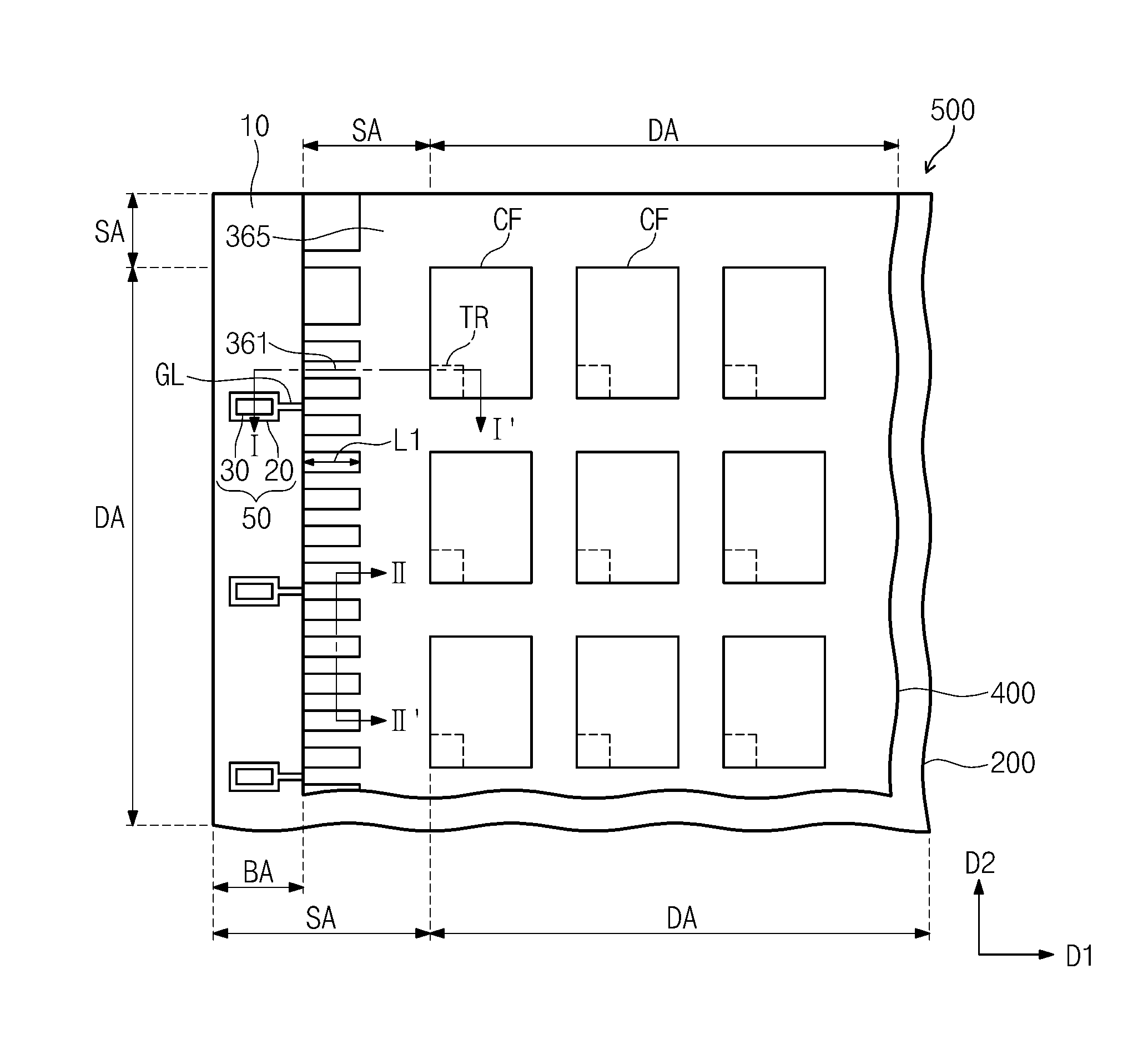
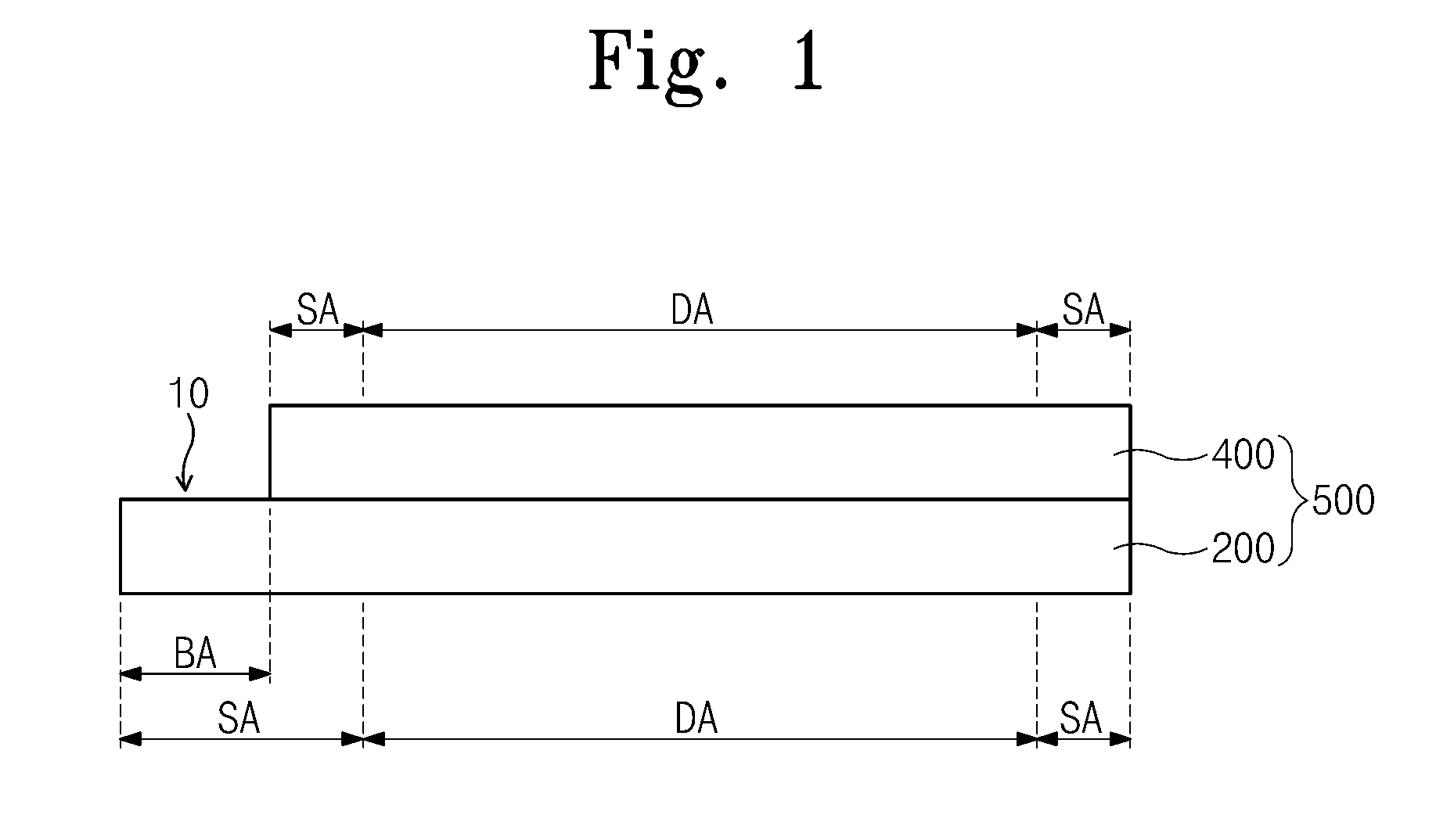
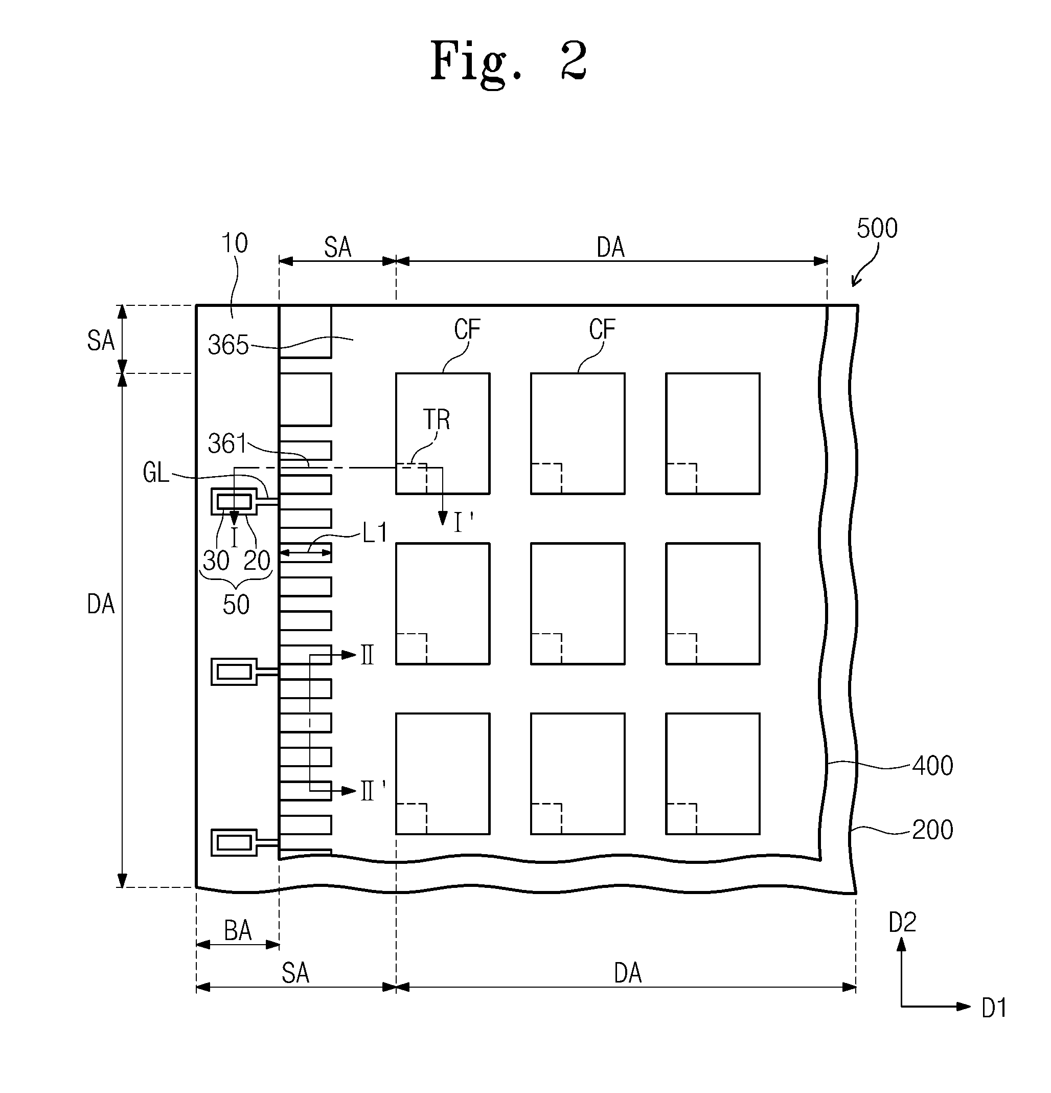
[0024]The invention is described more fully hereinafter with reference to the accompanying drawings, in which exemplary embodiments of the invention are shown. This invention may, however, be embodied in many different forms and should not be construed as limited to the exemplary embodiments set forth herein. Rather, these embodiments are provided so that this disclosure will be thorough and complete, and will fully convey the scope of the invention to those skilled in the art. In the drawings, the size and relative sizes of layers and regions may be exaggerated for clarity.

[0025]It will be understood that when an element or layer is referred to as being “on”, “connected to” or “coupled to” another element or layer, it can be directly on, connected or coupled to the other element or layer or intervening elements or layers may be present. In contrast, when an element is referred to as being “directly on,”“directly connected to” or “directly coupled to” another element or layer, there...


PUM

PropertyMeasurementUnit
lengthaaaaaaaaaa
lengthaaaaaaaaaa
widthaaaaaaaaaa

Abstract

In a method of manufacturing a display apparatus, an opposite substrate on which a conductive pattern is formed is coupled with a display substrate to face the display substrate, and the opposite substrate is cut to partially expose the display substrate. Since the conductive pattern is cut with the opposite substrate during the cutting of the opposite substrate, an electric resistance of the conductive pattern is changed. The change in electric resistance of the conductive pattern is detected to determine whether the opposite substrate is cut or not.

Description

[0001]This application claims priority to Korean Patent Application No. 10-2009-0008531 filed on Feb. 3, 2009, and all the benefits accruing therefrom under 35 U.S.C. §119, the contents of which are herein incorporated by reference in its entirety.BACKGROUND OF THE INVENTION[0002]1. Field of the Invention[0003]The present invention relates to a display apparatus and a method of manufacturing the same. More particularly, the present invention relates a display apparatus capable of preventing defects in manufacturing process and a method of manufacturing the display apparatus.[0004]2. Description of the Related Art[0005]Among flat panel displays, a flexible display indicates a display device which is flexibly bendable. The flexible display includes a plastic substrate having a thickness of about 0.2 millimeters (mm) which imparts flexibility to the display device, rather than a glass substrate of a relatively hard material which imparts rigidity.[0006]When manufacturing the flat panel...

Claims


Application Information

Patent Timeline
Patent Type & Authority Applications(United States)
IPC IPC(8): G02F1/1345H01J9/20H01J9/42
CPCB23K26/08B23K26/367B23K26/38B23K26/409B23K2201/18G02F2201/121G02F1/1303G02F1/1333G02F1/133305G02F2001/133388B23K2201/40B23K26/364B23K26/40B23K2101/18B23K2101/40B23K2103/172G02F1/133388G02F1/1345C03B33/02G02F1/13
Inventor PARK, JUNG WOO
Owner SAMSUNG ELECTRONICS CO LTD
Why Eureka
Try Eureka