
Method of manufacturing substrate for liquid discharge head
- Summary
- Abstract
- Description
- Claims
- Application Information
AI Technical Summary
Benefits of technology
Problems solved by technology
Method used
Image

Examples
first embodiment
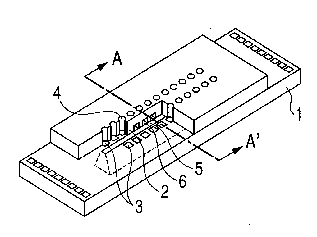
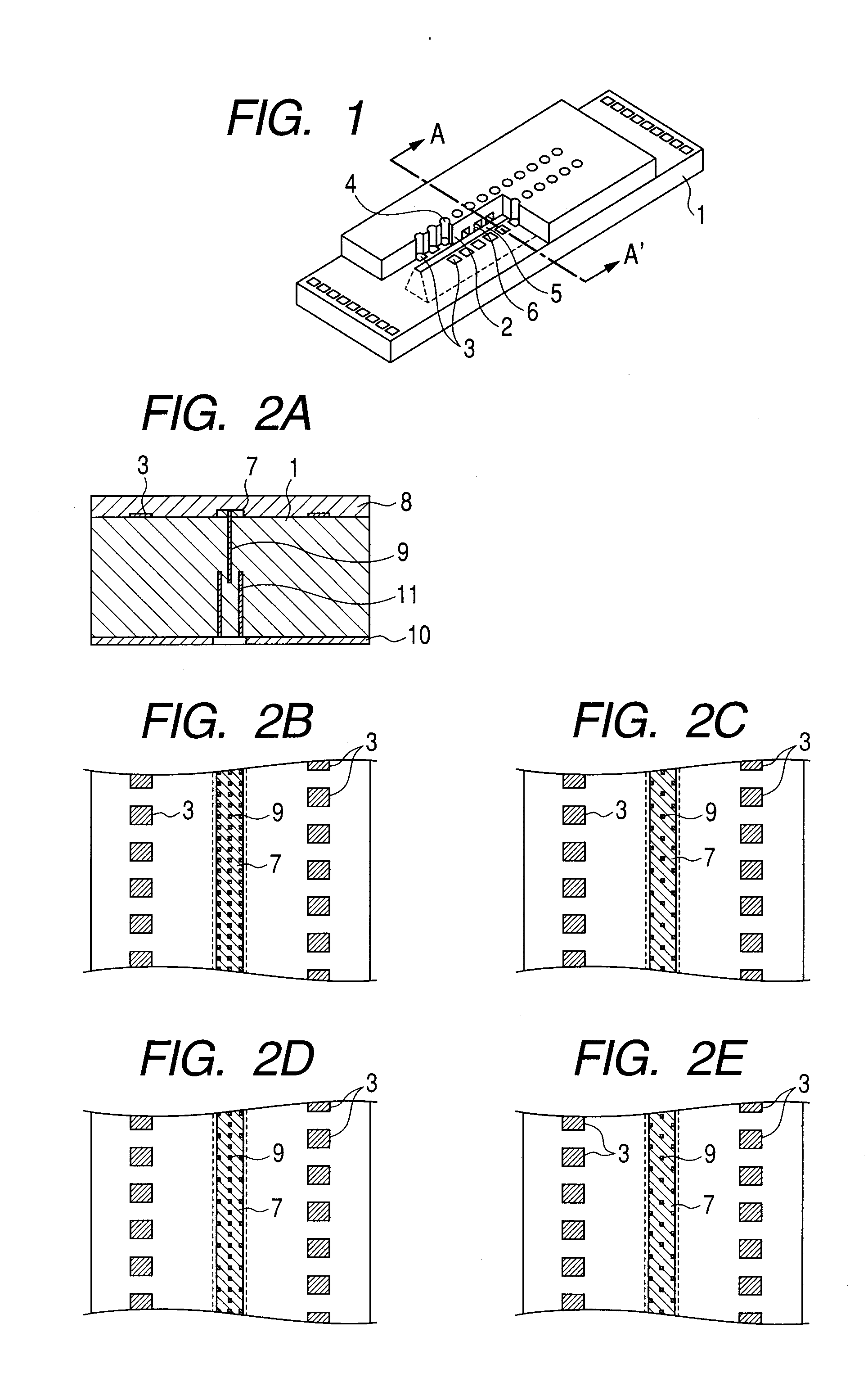
[0023]A portion of the liquid discharge head of one embodiment of the invention is shown in FIG. 1.
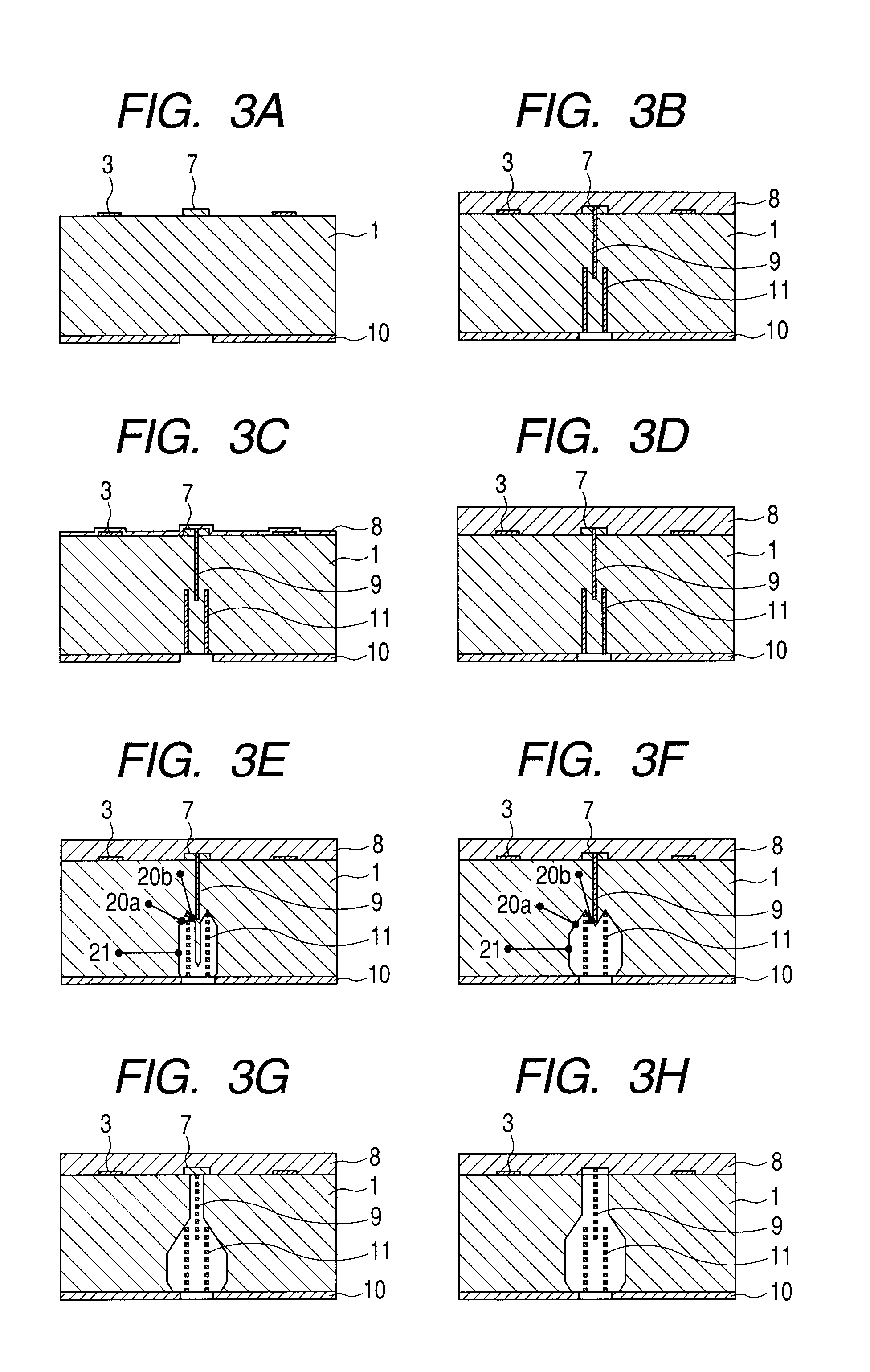
[0024]This liquid discharge head has a silicon substrate 1 in which two rows of liquid discharge energy generating elements (hereinafter referred to as energy generating elements) 3 are aligned and formed at predetermined pitches. On the silicon substrate 1, liquid discharge ports 4, which are opened above a flow passage side wall 2 and the energy generating elements 3, are formed from a coating photosensitive resin which forms a flow passage forming member. Upper portions of flow passages 6 which communicate with the liquid discharge ports 4 through the flow passages 6 from the liquid supply ports 5 are formed by this flow passage forming member. Additionally, the liquid supply ports 5 formed by the anisotropic etching of silicon are opened between two rows of the liquid discharge energy generating elements 3. This liquid discharge head applies the energy generated by an energy genera...
second embodiment
[0046]Next, the process of etching in the case the leading holes 9 of the front face of the silicon substrate 1 and the leading holes 11 of the rear face of the silicon substrate 1 do not overlap each other in the thickness direction of the silicon substrate 1 is shown in FIGS. 8A to 8H. In addition, in the following description, the steps of forming flow passages and discharge ports on a substrate are illustrated together.
[0047]As shown in FIG. 8A, the energy generating elements 8 and the sacrificial layer 7 are formed on the silicon substrate 1, and the etching mask 10 is formed on the face opposite to the front face of the silicon substrate 1. Thereafter, as shown in FIG. 8B, one row of the leading holes 9 are formed at pitches of 100 μm in the longitudinal direction of the opening of the front face, and the etching stop layer 12 of an organic film is patterned. As a specific example of the material, polymethylisopropenylketone (ODUR-1010 made by Tokyo Ohka Kogyo Co., Ltd.) is ex...
PUM
 Abstract
Description
Claims
Application Information