Substrate etching method and corresponding processing device

A technology for processing devices and substrates, which is applied in the manufacture of discharge tubes, electrical components, semiconductors/solid-state devices, etc., can solve the problems of cost reduction, distortion, and high cost, and achieve a good effect of chemical bombardment

Active Publication Date: 2019-03-05
ADVANCED MICRO FAB EQUIP INC CHINA
View PDF6 Cites 1 Cited by
  • Summary
  • Abstract
  • Description
  • Claims
  • Application Information

AI Technical Summary

Problems solved by technology

[0005] As a new generation of memory, 3D NAND devices are composed of several layers of etched materials, that is, amorphous carbon layers. Several holes for placing conductive materials are formed in the amorphous carbon layers. These holes are densely distributed, and the hole openings occupy The larger the area, the higher the cost; in the prior art, oxygen plasma etching is used, and the dielectric anti-reflection layer is used as a mask to etch the amorphous carbon layer below it, and the holes etched by this method The side is actually bow-shaped (low-like), and the mouth of the opening is larger than ideal and even produces distortion and aliasing, such as figure 1 As shown,

Method used


Image

  • Substrate etching method and corresponding processing device
  • Substrate etching method and corresponding processing device
  • Substrate etching method and corresponding processing device

Examples


Embodiment Construction

[0040] The present invention will be further elaborated below by describing a preferred specific embodiment in detail in conjunction with the accompanying drawings.

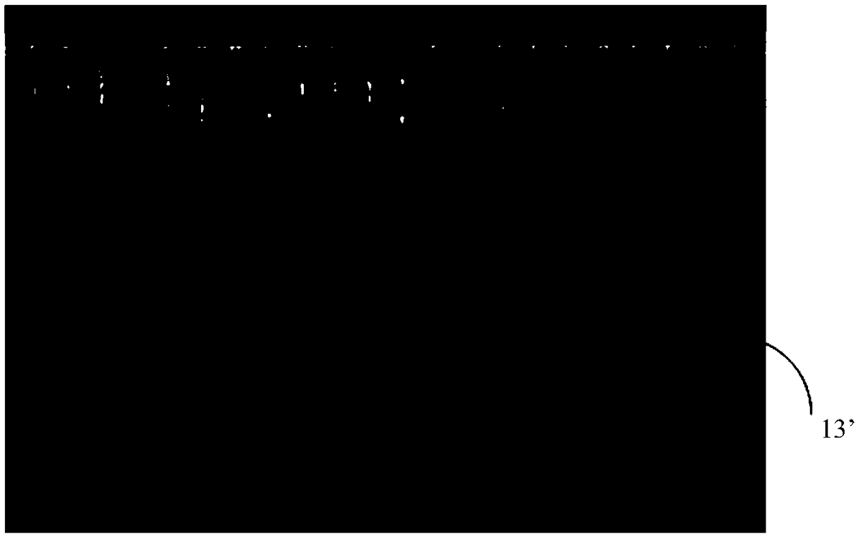
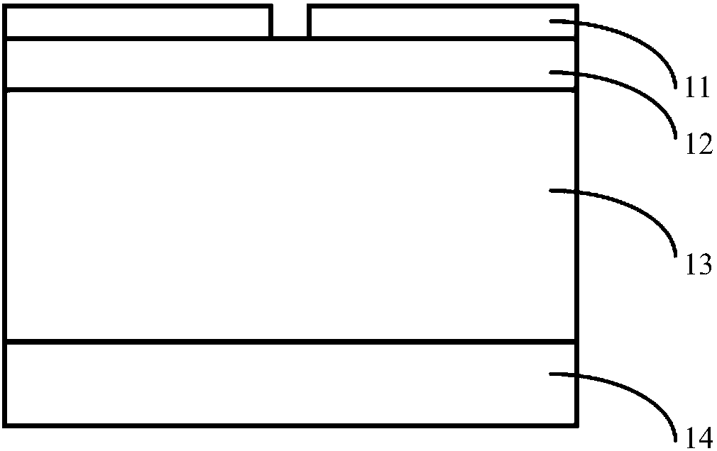
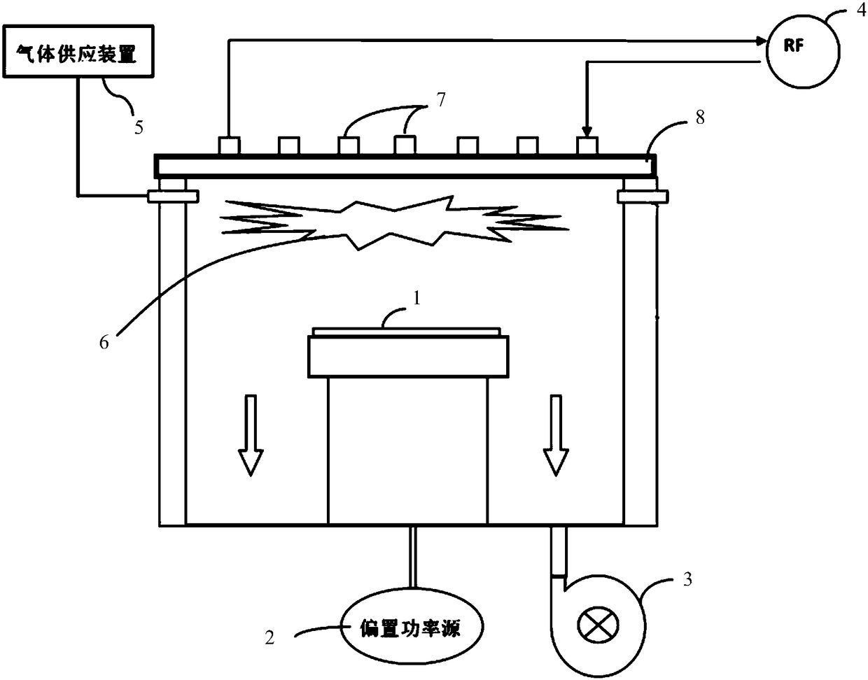
[0041] The invention discloses a method for etching a substrate. The structure of the substrate 1 etched by the etching method is as follows: figure 2 As shown, it includes a photoresist mask layer 11 , a dielectric antireflection layer 12 , a carbon hard mask layer 13 and a silicon oxide layer 14 . The etching method is carried out in a plasma processing device, and the plasma processing device is an inductively coupled plasma processing device or a capacitively coupled plasma processing device. For ease of description, image 3 An inductively coupled plasma reaction device is shown, including a vacuum reaction chamber, the vacuum reaction chamber includes a substantially cylindrical side wall made of metal material, an insulating window 8 is arranged above the side wall of the reaction chamber, and above the ...


PUM


Abstract

The invention provides a substrate etching method. The method is performed in a plasma processing device. A substrate etched by the substrate etching method comprises a photoresist mask layer, a dielectric anti-reflection layer, a carbon hard mask layer, and a silicon oxide layer, wherein the carbon hard mask layer below the dielectric anti-reflection layer is etched with a patterned dielectric anti-reflection layer as a mask so as to form a patterned carbon hard mask layer, the plasma processing device comprises an RF source power source and an RF bias power source, the RF bias power source outputs an RF signal with frequency greater than 2MHZ when the dielectric anti-reflection layer is etched, so as to monitor etching process, when etching of the dielectric anti-reflection layer is completed, an output frequency of the RF bias power source is switched to less than 2MHZ, so as to realize etching of the carbon hard mask layer. The method has the advantages of ensuring that an etchinghole wall of the carbon mask layer is vertical and lowering opening width of an etching hole.

Description

technical field [0001] The invention relates to the technical field of semiconductor manufacturing, in particular to a substrate etching method and a corresponding processing device. Background technique [0002] In the semiconductor integrated circuit manufacturing process, a semiconductor structure is formed on a semiconductor substrate through a series of processes, such as deposition, photolithography, etching, planarization and other processes. Wherein, a photolithography process is used to form a mask pattern to define a region to be etched. The etching process is used to transfer the pattern defined by lithography to the material (metal, dielectric layer or silicon) to form the desired structure. In the current semiconductor process, in order to enhance the accuracy of the transfer, it is generally used to first The pattern formed by the photoresist layer is transferred to the dielectric anti-reflection layer (or anti-reflection layer DARC) by exposure, and then the ...

Claims


Application Information

Patent Timeline
IPC IPC(8): H01L21/027H01L21/033H01L21/311H01J37/32
CPCH01J37/321H01J2237/3343H01L21/0274H01L21/0335H01L21/31116H01L21/31138
Inventor 严利均刘身健李洋饭塚浩
Owner ADVANCED MICRO FAB EQUIP INC CHINA
Why Eureka
Try Eureka