

Symmetric quadrupole structured field emission display without spacer
a structured field and display technology, applied in the direction of discharge tube luminescnet screen, discharge tube/lamp details, cathode ray tube/electron beam tube, etc., can solve the problem of limiting the use of high-voltage phosphors and the enhancement of lightness, poor gray-scale reproduction, and rapid aging of phosphors, etc. problem, to achieve the effect of low adjusting voltage, low cost and simple fabrication process
- Summary
- Abstract
- Description
- Claims
- Application Information
AI Technical Summary
Benefits of technology
Problems solved by technology
Method used
Image

Examples
Embodiment Construction
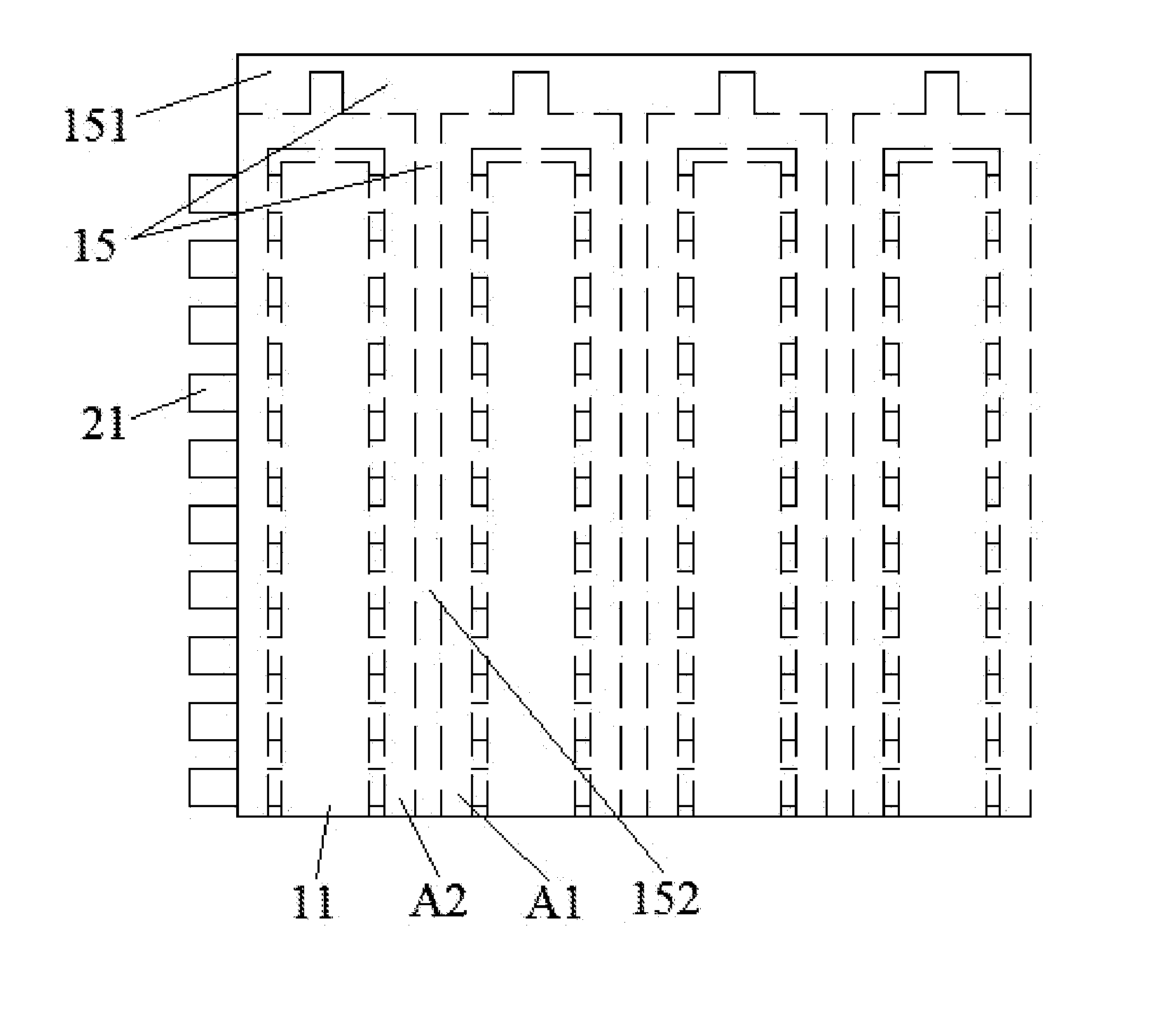
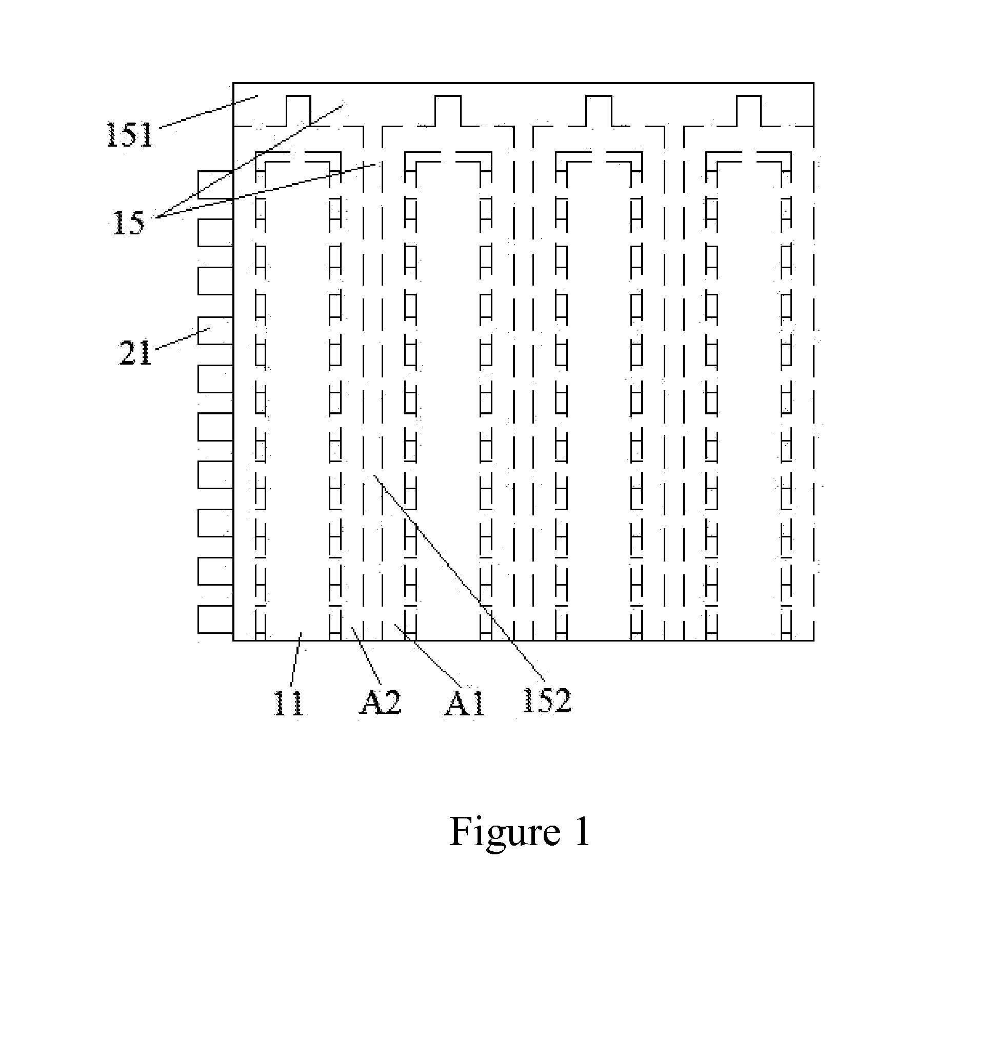
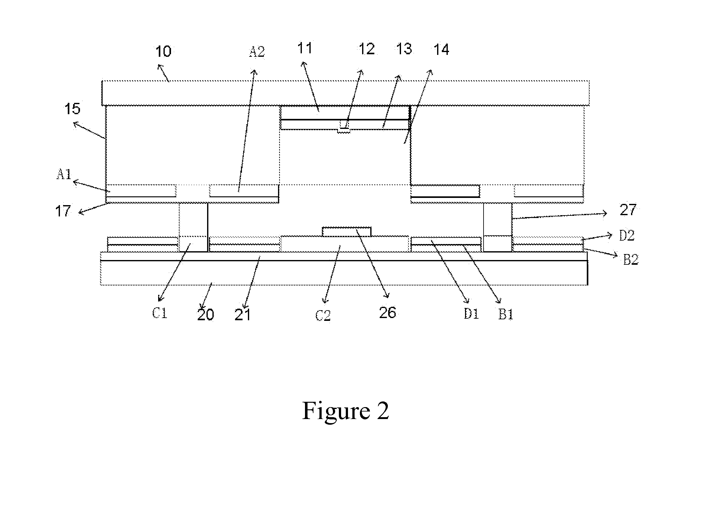
[0037]As shown in FIG. 1-4, the symmetric quadrupole structured field emission display without spacer, comprising two parallel substrates: upper substrate 10 and under substrate 20, which are adapted in the size, wherein a number of longitudinal strips of anode electrodes 11 are settled on the underside of the upper substrate 10 side by side, the bus electrodes 12 are settled on the anode 11 along the longitudinal centerline, phosphor layer 13 and anode dielectric layer 14 are settled on the anode 11 and bus electrode 12 along the longitudinal alternating, comb-like dielectric layer 15 is settled on the underside of the upper substrate 10, the comb-like dielectric layer 15 is composed of lateral connection belts 151 that are arranged in the flanking on the upper substrate 10 and a number of longitudinal work belts 152 that are arranged side by side on one side of the lateral connection belts 151, the longitudinal work belts 152 and the anodes 11 are parallel, and are arranged on the...
PUM
 Abstract
Description
Claims
Application Information