Image sensor and method for fabricating the same

Active Publication Date: 2015-05-14
SK HYNIX INC
View PDF4 Cites 5 Cited by
  • Summary
  • Abstract
  • Description
  • Claims
  • Application Information

AI Technical Summary

Benefits of technology

The present invention is about an image sensor that can prevent problems such as dark current from affecting its quality. This patent describes a method to make this type of image sensor.

Problems solved by technology

Image sensors have a concern in that dark current may deteriorate characteristics of the image sensors.

Method used


Image

  • Image sensor and method for fabricating the same
  • Image sensor and method for fabricating the same
  • Image sensor and method for fabricating the same

Examples


Embodiment Construction

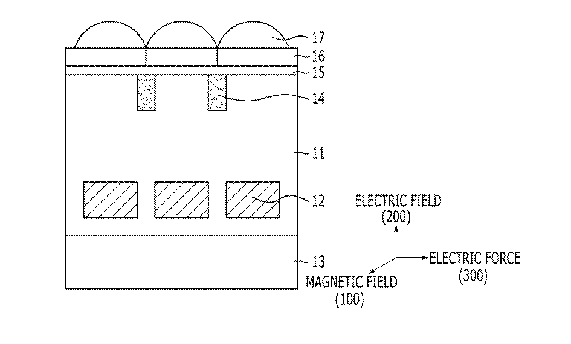
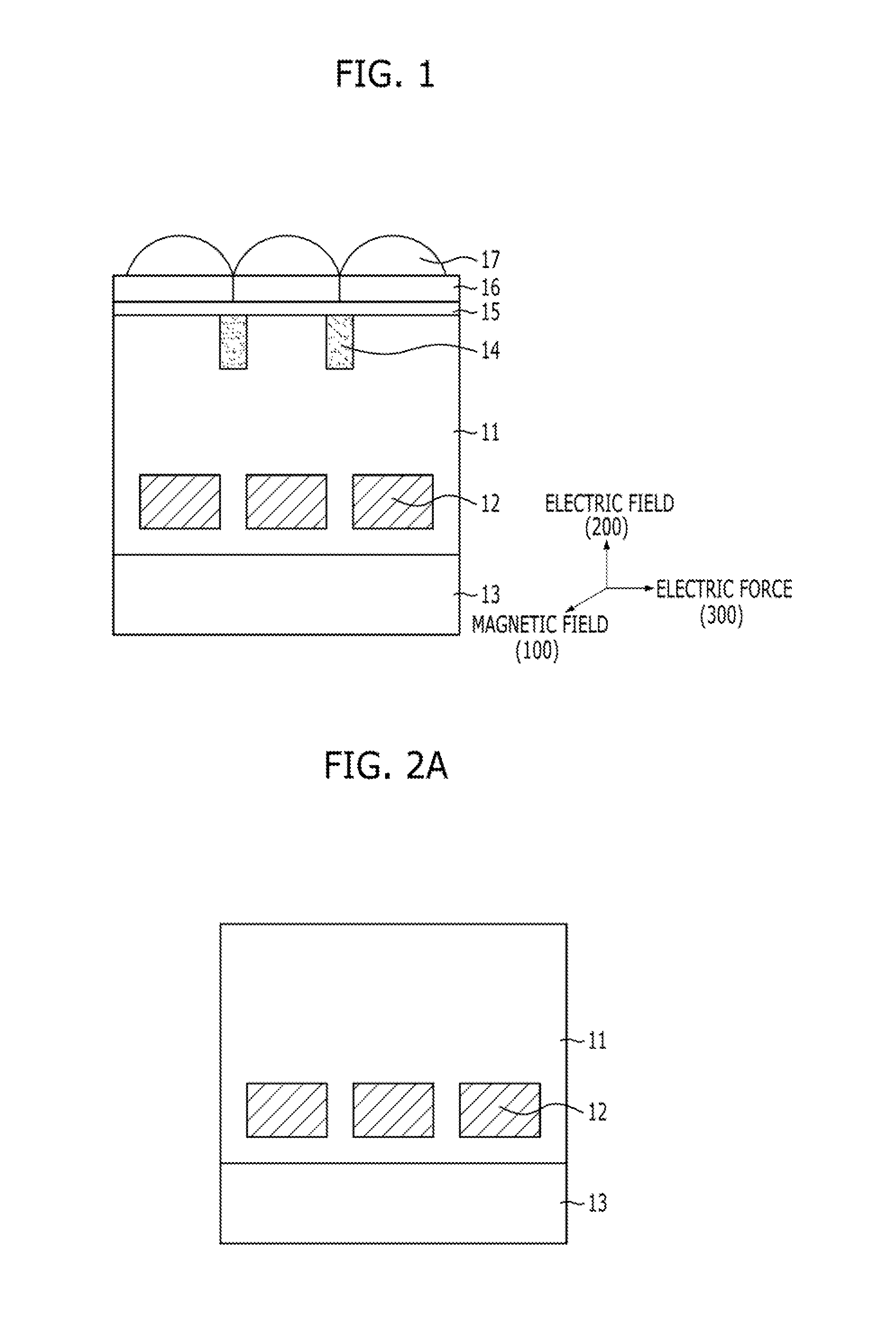
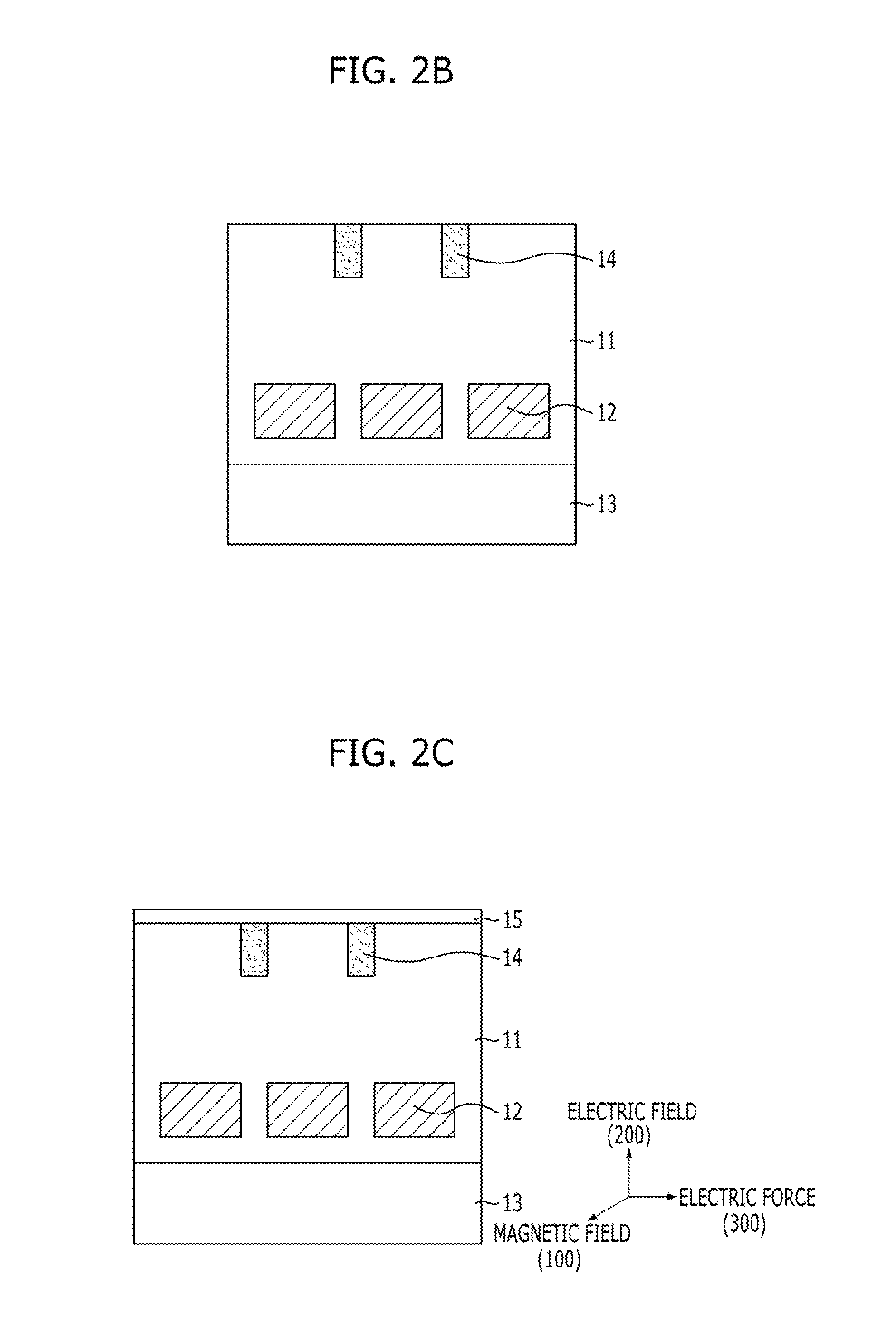
[0014]Exemplary embodiments of the present invention will be described below in more detail with reference to the accompanying drawings. The present invention may, however, be embodied in different forms and should not be construed as limited to the embodiments set forth herein. Rather, these embodiments are provided so that this disclosure will be thorough and complete, and will fully convey the scope of the present invention to those skilled in the art. Throughout the disclosure, reference numerals correspond directly to the like numbered parts in the various figures and embodiments of the present invention.

[0015]The drawings are not necessarily to scale and in some instances, proportions may have been exaggerated in order to dearly illustrate features of the embodiments. When a first layer is referred to as being “on” a second layer or “on” a substrate, it not only refers to a case where the first layer is formed directly on the second layer or the substrate but also a case where...


PUM


Abstract

An image sensor includes a substrate including photoelectric conversion regions, a magnetic layer disposed on a back side of the substrate and suitable for generating a magnetic field, and color filters and microlenses disposed on the magnetic layer.

Description

CROSS-REFERENCE TO RELATED APPLICATIONS[0001]The present application claims priority of Korean Patent Application No. 10-2013-0137656 on Nov. 13, 2013, which is incorporated herein by reference in its entirety.BACKGROUND[0002]1. Field[0003]Exemplary embodiments of the present invention relate to an image sensor, and more particularly, to a back side illumination image sensor and a method for fabricating the back side same.[0004]2. Description of the Related Art[0005]An image sensor transforms an optical image into electric signals. Generally, image sensors are categorized into a Charge Coupled Device (CCD) image sensor and a CMOS image sensor (CIS). An image sensor includes a plurality of pixels, and each of the pixels outputs a pixel signal corresponding to incident light. Herein, each of the pixels accumulates photocharges corresponding to incident light in a photoelectric converting device, which is represented by a photodiode, and outputs a pixel signal based on the accumulated ...

Claims


Application Information

Patent Timeline
IPC IPC(8): H01L27/146
CPCH01L27/14638H01L27/1464H01L27/14621H01L27/14627H01L27/14685H01L27/14601H01L27/146
Inventor KIM, DO-HWANWOO, DONG-HYUNKIM, JONG-CHAECHOI, CHUNG-SEOK
Owner SK HYNIX INC
Why Eureka
Try Eureka