

Duty cycle correction circuit
a duty cycle and circuit technology, applied in pulse manipulation, pulse duration/width modulation, pulse technique, etc., can solve problems such as data input/output at the incorrect tim
- Summary
- Abstract
- Description
- Claims
- Application Information
AI Technical Summary
Benefits of technology
Problems solved by technology
Method used
Image

Examples
Embodiment Construction
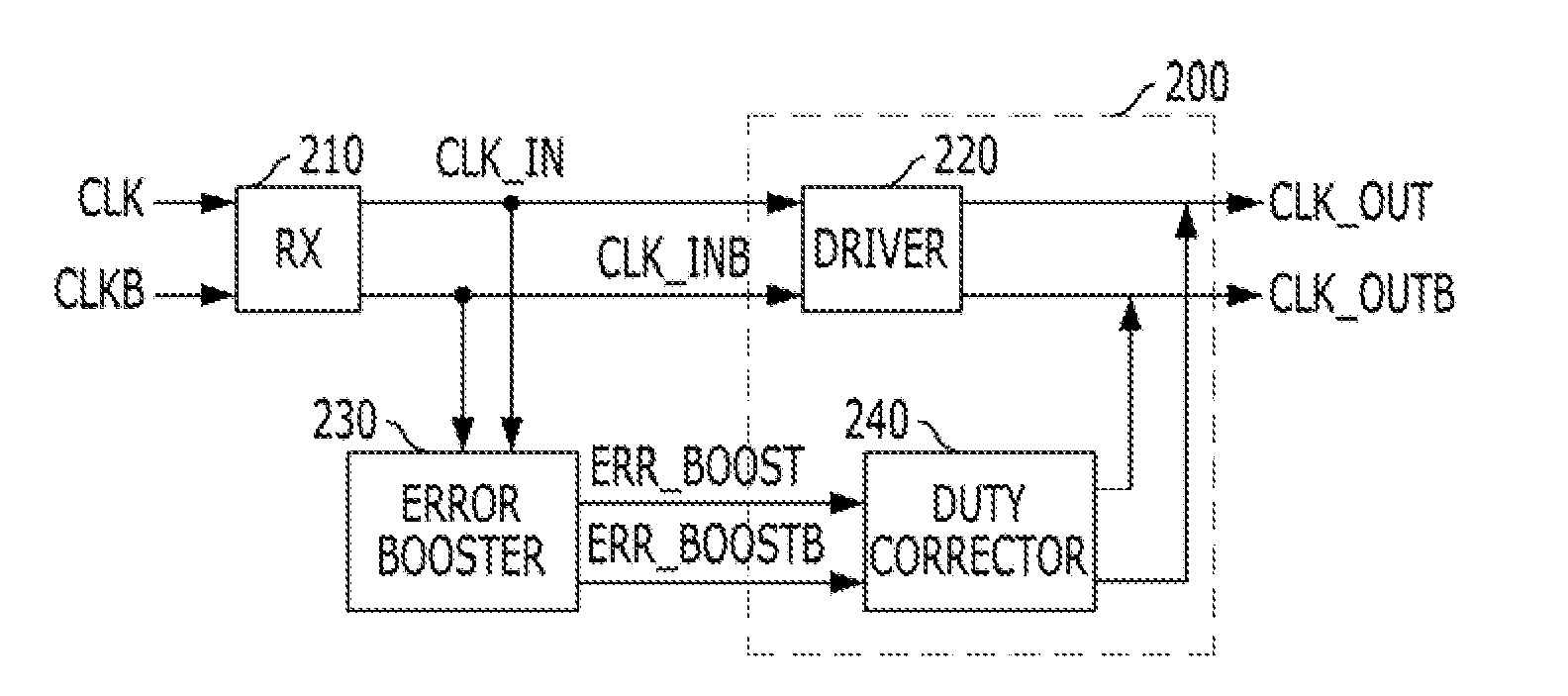
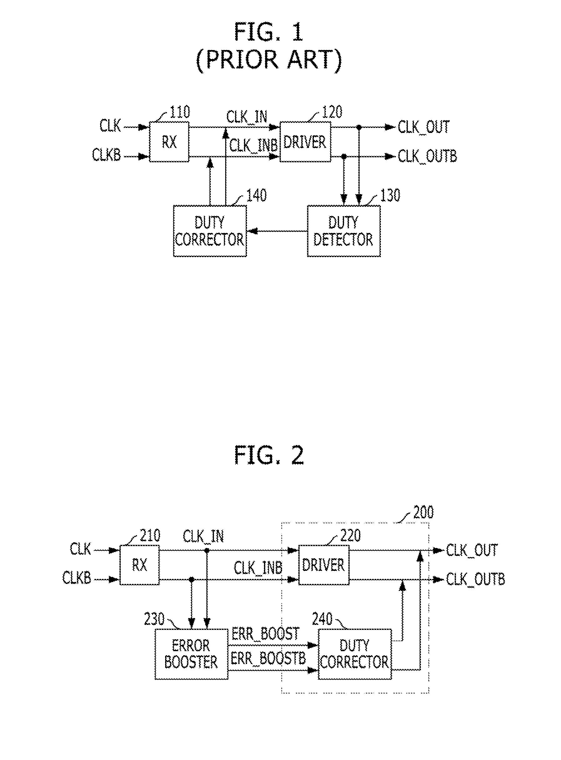
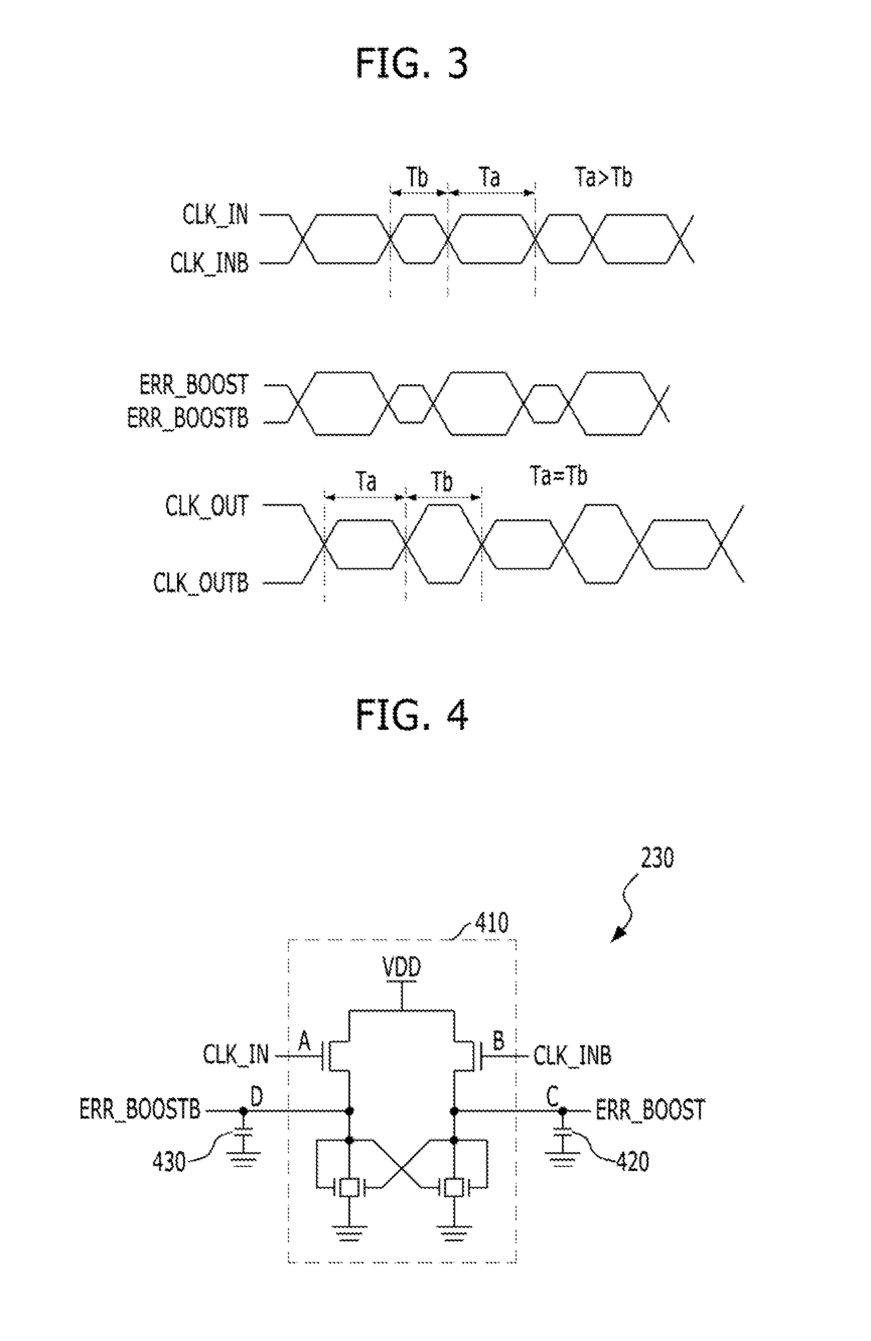
[0022]Various embodiments will be described below in detail with reference to the accompanying drawings. The present invention may, however, be embodied in different forms and should not be construed as limited to the embodiments set forth herein. Rather, these embodiments are provided so that this disclosure will be thorough and complete, and will fully convey the scope of the present invention to those skilled in the art. Throughout the disclosure, reference numerals correspond directly to the like numbered parts in the various figures and embodiments of the present invention.
[0023]The drawings are not necessarily to scale and, in some instances, proportions may have been exaggerated to clearly illustrate features of the embodiments.
[0024]In this specification, specific terms have been used. The terms are used to describe the present invention and are not used to qualify the sense or limit the scope of the present invention. It is also noted that in this specification, ‘and / or’ re...
PUM
 Abstract
Description
Claims
Application Information