Light-Emitting Device
a technology of light-emitting devices and light-emitting devices, which is applied in the direction of semiconductor devices, instruments, electrical devices, etc., can solve the problem that the original image data cannot be completely rewritten, and achieve the effect of reducing the writing frequency of image data and small off-state curren
- Summary
- Abstract
- Description
- Claims
- Application Information
AI Technical Summary
Benefits of technology
Problems solved by technology
Method used
Image

Examples
embodiment 1
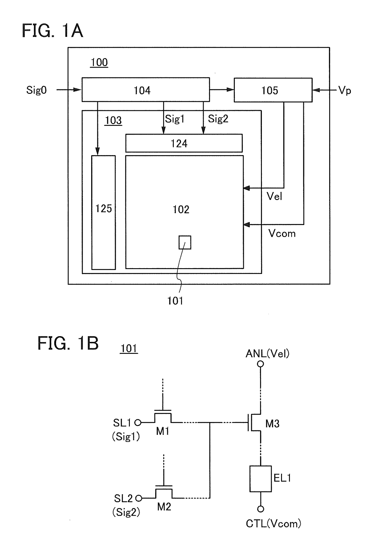
[0047]A configuration example of a light-emitting device according to one embodiment of the present invention is shown in a block diagram of FIG. 1A. Although the block diagram shows elements classified according to their functions in independent blocks, it may be practically difficult to completely separate the elements according to their functions and, in some cases, one element may be involved in a plurality of functions.
[0048]A light-emitting device 100 in FIG. 1A includes at least a panel 103 including a pixel portion 102 composed of a plurality of pixels 101, a signal line driver circuit (a source driver) 124, and a scan line driver circuit (a gate driver) 125; a controller 104, and a power supply circuit 105. Each of the pixels 101 includes a light-emitting element and a transistor for controlling operation of the light-emitting element.
[0049]When a signal Sig0 containing image data is input to the controller 104, the controller 104 has a function of processing the signal Sig...
embodiment 2
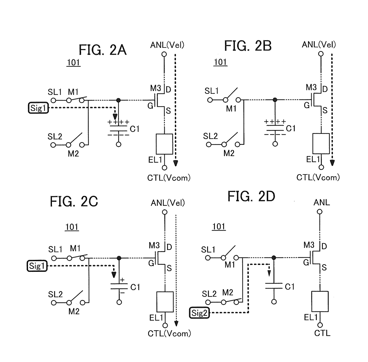
[0090]In this embodiment, one embodiment of the present invention will be described with reference to FIG. 9. One embodiment of the present invention is effective when the signal Sig1 is input at a high scan frequency, such as in double-frame rate driving. As the scan frequency is increased, the period for inputting the signal Sig1 is shortened, and a potential corresponding to the signal Sig1 is not completely input to a pixel in some cases. However, one embodiment of the present invention can solve the problem.
[0091]FIG. 9 is a timing chart of one embodiment the present invention, showing the case where a signal which is the same as the signal Sig1 is input as the signal Sig2 to the wiring SL2 only one GL-selected period earlier than the signal Sig1 is supplied to the wiring SL1. The data of the signal Sig1 and signal Sig2 are referred to as signals S1, S2, S3 to Sn in divided periods.
[0092]In the period p0 in FIG. 9, the signal S1 as the signal Sig2 is applied to the wiring SL2 w...
embodiment 3
[0097]In this embodiment, a structure example of the light-emitting device 100 illustrated in FIG. 1A is described in detail.
[0098]FIG. 10 is a block diagram illustrating a structure example of a light-emitting device according to one embodiment of the present invention. Like in FIG. 1A, the light-emitting device 100 in FIG. 10 includes the panel 103 including the pixel portion 102 composed of the plurality of pixels 101, the signal line driver circuit (a source driver) 124, and the scan line driver circuit (a gate driver) 125; the controller 104, and the power supply circuit 105. The light-emitting device 100 in FIG. 10 further includes the input device 120, the CPU 121, the image processing circuit 122, and the image memory 123.
[0099]The input device 120 has a function of applying data or an instruction to the CPU 121 included in the light-emitting device 100. For example, the input device 120 can apply an instruction to transfer the pixel portion 102 from an operation state to a ...
PUM
 Abstract
Description
Claims
Application Information
 - R&D Engineer
- R&D Manager
- IP Professional
- Industry Leading Data Capabilities
- Powerful AI technology
- Patent DNA Extraction
Browse by: Latest US Patents, China's latest patents, Technical Efficacy Thesaurus, Application Domain, Technology Topic.
© 2024 PatSnap. All rights reserved.Legal|Privacy policy|Modern Slavery Act Transparency Statement|Sitemap