Semiconductor device and method for manufacturing the same

Active Publication Date: 2019-02-28
SAMSUNG ELECTRONICS CO LTD
View PDF7 Cites 4 Cited by
  • Summary
  • Abstract
  • Description
  • Claims
  • Application Information

AI Technical Summary

Benefits of technology

[0004]In an aspect, a semiconductor device may include a substrate including a first region and a second region, memory transistors on the first region, a first interconnection layer on the memory transistors and including first interconnection lines, and a second interconnection layer on the first interconnection layer and including second interconnection lines. The second interconnection lines on the first region include a first line extending along a first direction and spaced from the second region by a first distance along the fir

Problems solved by technology

To satisfy these demands, semiconductor devices have been highly integrated

Method used


Image

  • Semiconductor device and method for manufacturing the same
  • Semiconductor device and method for manufacturing the same
  • Semiconductor device and method for manufacturing the same

Examples


Example

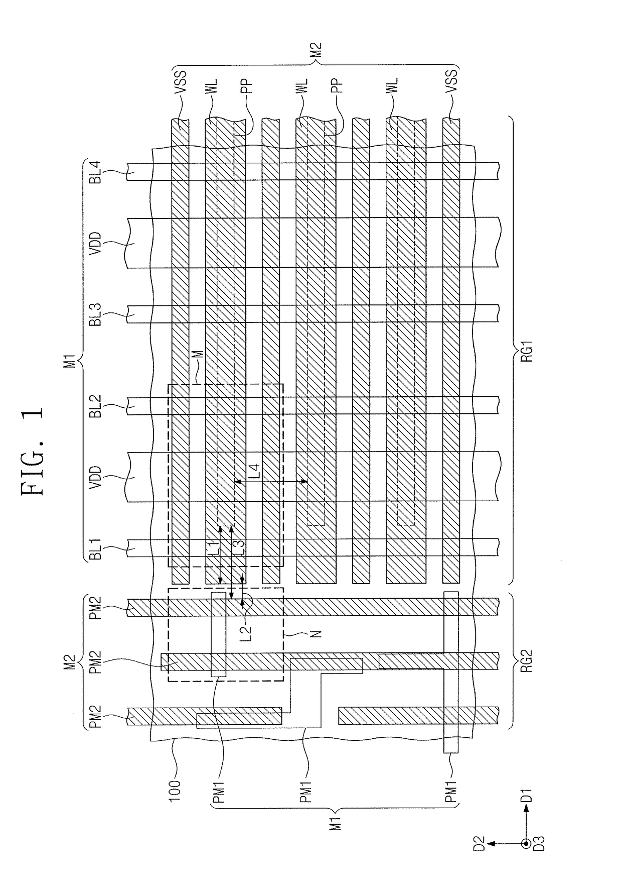
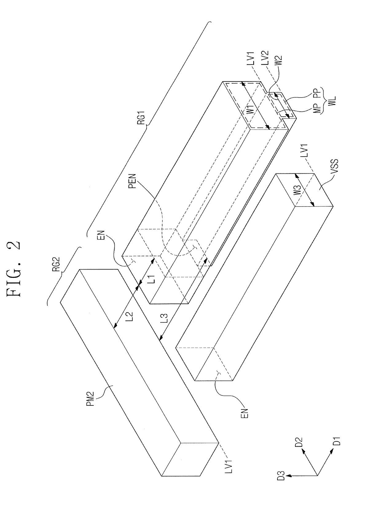
[0027]FIG. 1 is a plan view illustrating a semiconductor device according to some embodiments. FIG. 2 is a perspective view schematically illustrating second interconnection lines of FIG. 1.

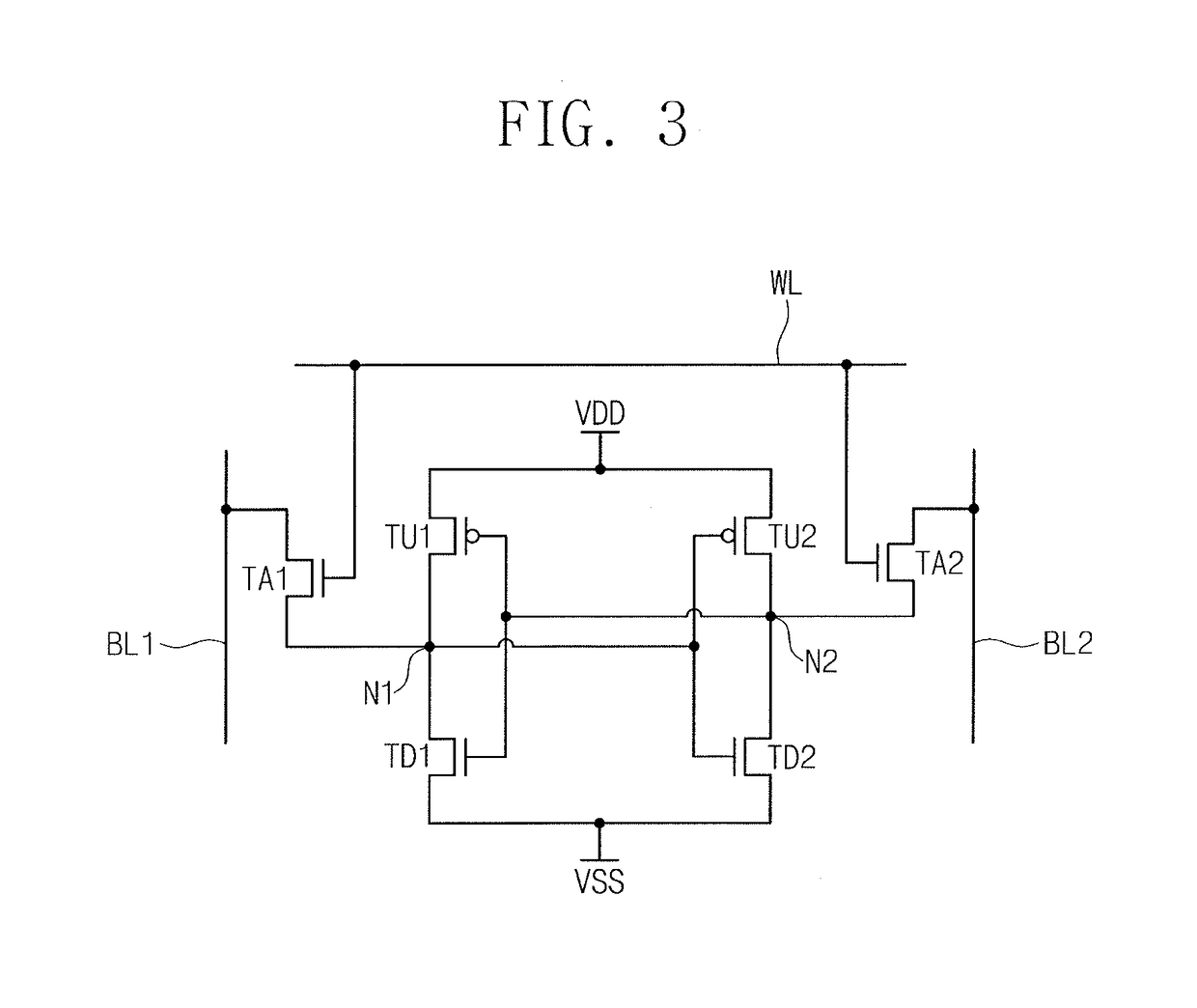
[0028]Referring to FIGS. 1 and 2, a substrate 100 including a first region RG1 and a second region RG2 may be provided. The first and second regions RG1 and RG2 may be adjacent to each other. The first region RG1 may be a memory cell region. For example, memory transistors constituting a static random access memory (SRAM) cell may be disposed on the first region RG1 of the substrate 100. The memory transistors and the SRAM cell including them will be described later in more detail.

[0029]The second region RG2 may be a logic cell region on which logic transistors constituting a logic circuit of a semiconductor device are disposed. For example, the logic transistors constituting a processor core or an input / output (I / O) terminal may be disposed on the second region RG2 of the substrate 100. The logi...


PUM


Abstract

A semiconductor device includes a substrate including a first region and a second region, memory transistors on the first region, a first interconnection layer on the memory transistors and including first interconnection lines, and a second interconnection layer on the first interconnection layer and including second interconnection lines. The second interconnection lines on the first region include a first line extending along a first direction and spaced from the second region by a first distance along the first direction, and a second line extending along the first direction, spaced from the first line along a second direction intersecting the first direction, and having a width smaller than that of the first line. The first line includes a protrusion extending along a third direction toward the substrate. The protrusion is spaced from the second region by a second distance along the first direction greater than the first distance.

Description

CROSS-REFERENCE TO RELATED APPLICATION[0001]Korean Patent Application No. 10-2017-0106194, filed on Aug. 22, 2017, in the Korean Intellectual Property Office, and entitled: “Semiconductor Device and Method for Manufacturing the Same,” is incorporated by reference herein in its entirety.BACKGROUND1. Field[0002]Embodiments relate to a semiconductor device and a method for manufacturing the same and, more particularly, to a semiconductor device including interconnection lines disposed on memory transistors of a substrate and a method for manufacturing the same.2. Description of the Related Art[0003]Semiconductor devices are widely used in an electronic industry because of their small sizes, multi-functional characteristics, and / or low manufacture costs. Semiconductor devices may be categorized as any one of semiconductor memory devices storing logical data, semiconductor logic devices processing logical data, and hybrid semiconductor devices having both the function of the semiconducto...

Claims


Application Information

Patent Timeline
IPC IPC(8): H01L27/02H01L27/11H01L27/092H01L23/528H01L23/522H01L21/8238H01L21/027H01L21/768
CPCH01L27/0207H01L27/1104H01L27/1116H01L27/092H01L23/5283H01L23/5286H01L23/5226H01L21/823871H01L21/0274H01L21/76816H01L21/76877H10B10/12H01L21/823807H01L21/76811H01L29/772H10B10/18
Inventor JEONG, LAKGYOYANG, SEOLUNCHO, YONGRAEHONG, HEE BUM
Owner SAMSUNG ELECTRONICS CO LTD
Why Eureka
Try Eureka