Display device

a liquid crystal display and display panel technology, applied in the direction of static indicating devices, instruments, etc., can solve the problems of non-uniform offset, display panel defects of flashing and residual image, and ignore voltage offset, so as to achieve the effect of reducing the voltage offset of the pixel voltage and achieving high performan

Inactive Publication Date: 2020-02-13
HKC CORP LTD
View PDF0 Cites 1 Cited by
  • Summary
  • Abstract
  • Description
  • Claims
  • Application Information

AI Technical Summary

Benefits of technology

[0030]It is unavoidable to form parasitic capacitance between the gate and the drain of the thin-film transistor. When the scan signal rises or falls suddenly, the thin-film transistor is turned off immediately, so that the voltage of the pixel electrode (hereafter refer to as a pixel voltage) is decreased in response to the rising offset and the falling offset of the scan signal caused by the parasitic capacitance. The rising offset or the falling offset is generated by subtracting the non-scan voltage from the scan voltage. As a result, the pixel voltage having a significant voltage offset may cause the image flashing and the display degradation problem. However, the display device of the present disclosure is able to control the rising part and the falling part of the scan signal to prevent the scan signal from suddenly rising or falling, so as to reduce the voltage offset of the pixel voltage caused by parasitic capacitance.
[0031]Furthermore, the conductive lines disposed on the transparent insulate substrate, made by glass, are not ideal paths, so the signals transmitted on the conductive lines may be delayed. The structure of the display device of the present disclosure can prevent from nonuniform display due to signal delay, and the voltage offsets of the pixel voltages caused by parasitic capacitance can be reduced to become more uniform. As a result, the display image with high performance can be obtained.

Problems solved by technology

The parasitic capacitance inside the display panel causes non uniform offsets of the pixel voltages in entire display panel; furthermore, when the LCD device has a larger screen and higher resolution, it is hard to ignore the voltage offsets caused by transmission delay.
As a result, a conventional solution of biasing a common voltage is unable to absorb the differences between the voltage offsets in entire display panel, and the pixels of the display panel cannot be driven by AC field optimally, so that the display panel may have the defects of flashing and residual image because of applying the AC field.
It is unavoidable to form parasitic capacitance between the gate and the drain of the thin-film transistor.
As a result, the pixel voltage having a significant voltage offset may cause the image flashing and the display degradation problem.
Furthermore, the conductive lines disposed on the transparent insulate substrate, made by glass, are not ideal paths, so the signals transmitted on the conductive lines may be delayed.

Method used


Image

  • Display device
  • Display device
  • Display device

Examples


Embodiment Construction

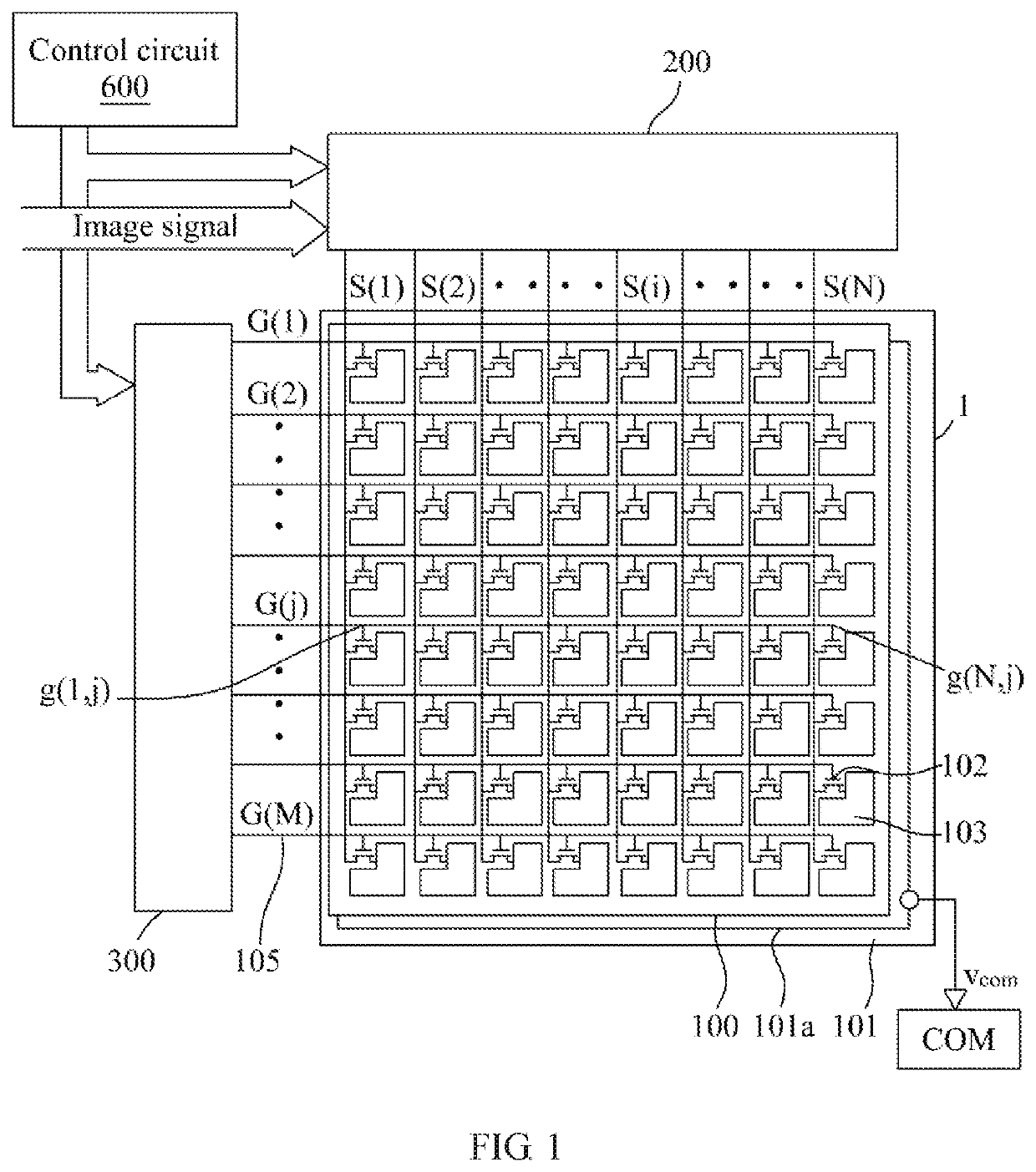
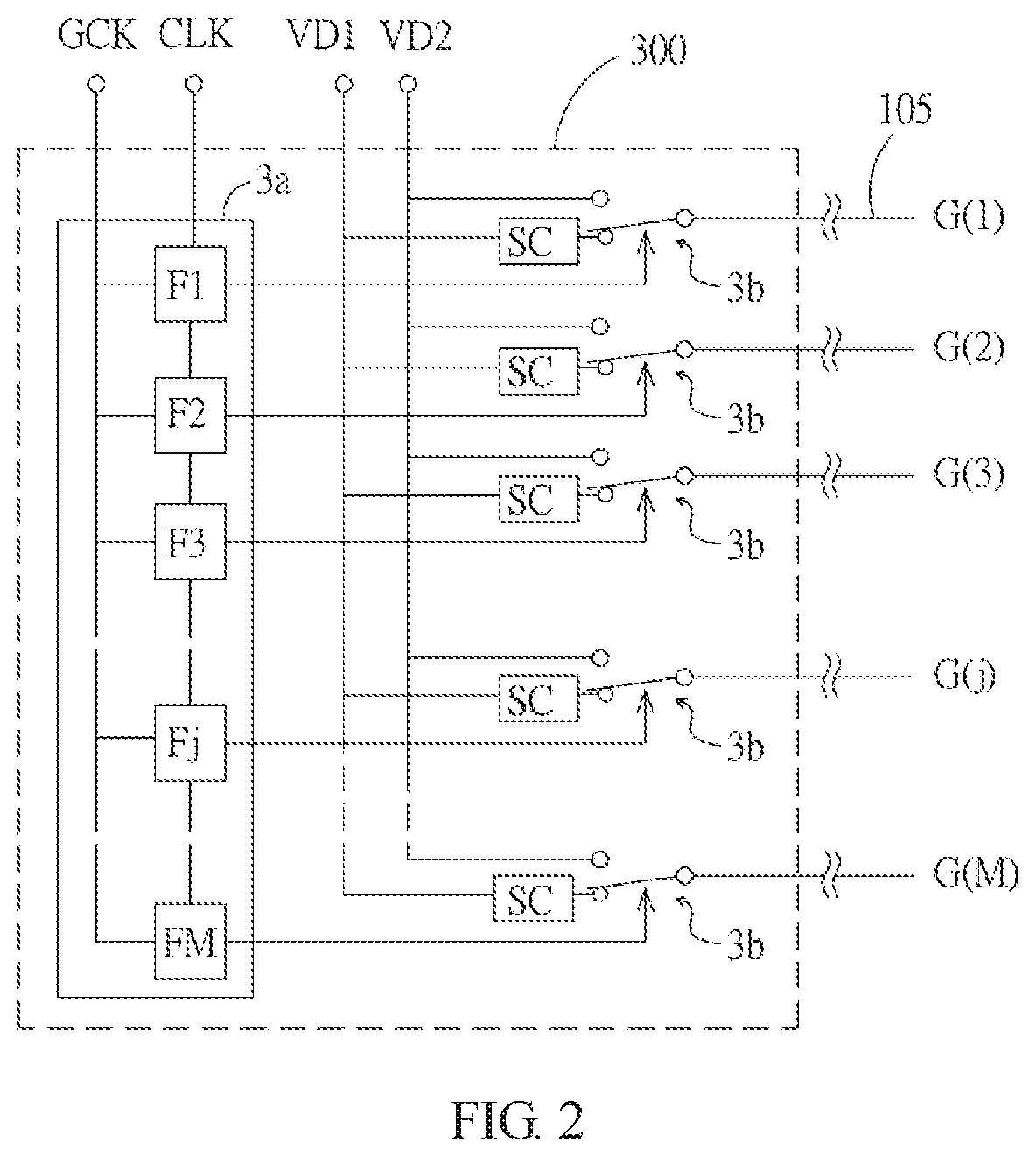
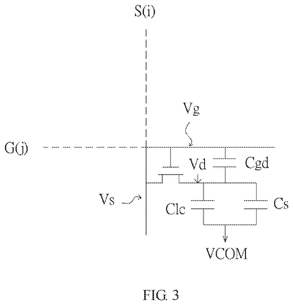
[0053]The following embodiments of the present disclosure are herein described in detail with reference to the accompanying drawings. These drawings show specific examples of the embodiments of the present disclosure. It is to be understood that these embodiments are exemplary implementations and are not to be construed as limiting the scope of the present disclosure in any way. Further modifications to the disclosed embodiments, as well as other embodiments, are also included within the scope of the appended claims. These embodiments are provided so that this disclosure is thorough and complete, and fully conveys the inventive concept to those skilled in the art. Regarding the drawings, the relative proportions and ratios of elements in the drawings may be exaggerated or diminished in size for the sake of clarity and convenience. Such arbitrary proportions are only illustrative and not limiting in any way. The same reference numbers are used in the drawings and description to refer...


PUM


Abstract

The disclosure illustrates a display device comprising: pixels arranged in a matrix form; image signal lines providing data signals to the pixels; scan signal lines crossing the image signal lines; a gate driver circuit configured to output a scan signal to the plurality of scan signal lines, and drive the scan signal lines by the scan signal; and a control circuit configured to control the gate driver circuit through a control signal comprising voltage waveform with voltage variation cycles. When a scan cycle of the scan signal is started, a voltage level of the scan signal non-vertically rises from a first voltage level to a second voltage level, and the voltage level of the scan signal is maintained at the second voltage levels, and when the scan cycles is ended, the voltage level of the scan signal non-vertically falls from the second voltage level to the first voltage level.

Description

CROSS-REFERENCE TO RELATED APPLICATION[0001]This application claims the benefit of China Patent Application No. 201711022782.9, filed on Oct. 26, 2017, in the State Intellectual Property Office of the People's Republic of China, the disclosure of which is incorporated herein in its entirety by reference.BACKGROUND1. Field[0002]The present disclosure relates to the matrix-type liquid crystal display device and a display method thereof, more particularly to a display device (such as a LCD device) and a display method, and each display pixel of display device includes thin-film transistors served as switch devices.2. Description of the Related Art[0003]The LCD devices are widely applied to many display devices such as television or graphic display device. Each display pixel include a thin-film transistor (hereafter refer to as TFT) served as a switch device, so that the adjacent display pixels are not interfered with each other, thereby preventing a crosstalk image under a condition th...

Claims


Application Information

Patent Timeline
Patent Type & Authority Applications(United States)
IPC IPC(8): G09G3/36
CPCG09G2320/0257G09G3/3648G09G2320/0219G09G2320/0247G09G3/3696G09G3/3677G09G2310/0259G09G2310/066G09G2320/0223
Inventor SHAN, JIANFENG
Owner HKC CORP LTD
Why Eureka
Try Eureka