Metal oxide thin film transistor

a thin film transistor and metal oxide technology, applied in the field of thin film transistors, can solve the problems of limiting the development of high-quality flat panel displays, the operating speed of tft b, etc., and achieve the effects of shortening the length of the gate electrode, reducing the density of the carrier and mobility, and accelerating the operating speed of

Active Publication Date: 2015-09-22
E INK HLDG INC
View PDF19 Cites 0 Cited by
  • Summary
  • Abstract
  • Description
  • Claims
  • Application Information

AI Technical Summary

Benefits of technology

[0020]In view of the description above, by utilizing the aforementioned metal oxide TFT, the defects present in a conventional amorphous silicon TFT such as low carrier density and mobility can be eliminated, and the operating speed of the TFT can be accelerated. In addition, by shortening the length of the gate electrode or by lengthening the interval between the source and the drain electrodes, overlapping between the orthographic projection of the source electrode on the substrate and the gate electrode and / or between the orthographic projection of the drain electrode on the substrate and the gate electrode is eliminated. Thus, the stability of a threshold voltage of the TFT can be improved, and the parasitic capacitance between the drain electrode and the gate electrode can be minimized. Accordingly, the capacitance coupling effect between the pixel units and the scan lines in the flat panel display can be also minimized, such that voltage shifts of the pixel units when the TFTs are switching on and off can be decreased, ultimately allowing for the image quality of the flat panel display to be improved.

Problems solved by technology

Moreover, the low carrier density and carrier mobility in the amorphous silicon also limit the operating speed of the TFT 100, and therefore place limitations on the development of high-quality flat panel displays.

Method used


Image

  • Metal oxide thin film transistor
  • Metal oxide thin film transistor
  • Metal oxide thin film transistor

Examples


Embodiment Construction

[0029]In the following detailed description, for purposes of explanation, numerous specific details are set forth in order to attain a thorough understanding of the disclosed embodiments. It will be apparent, however, that one or more embodiments may be practiced without these specific details. In other instances, well-known structures and devices are schematically shown in order to simplify the drawing.

[0030]The embodiments of the invention provide a metal oxide TFT to solve the problem of low operating speed in a conventional TFT, and also to solve the problem of an excessive increase in the threshold voltage shift of the metal oxide TFT after the metal oxide TFT is bias stressed.

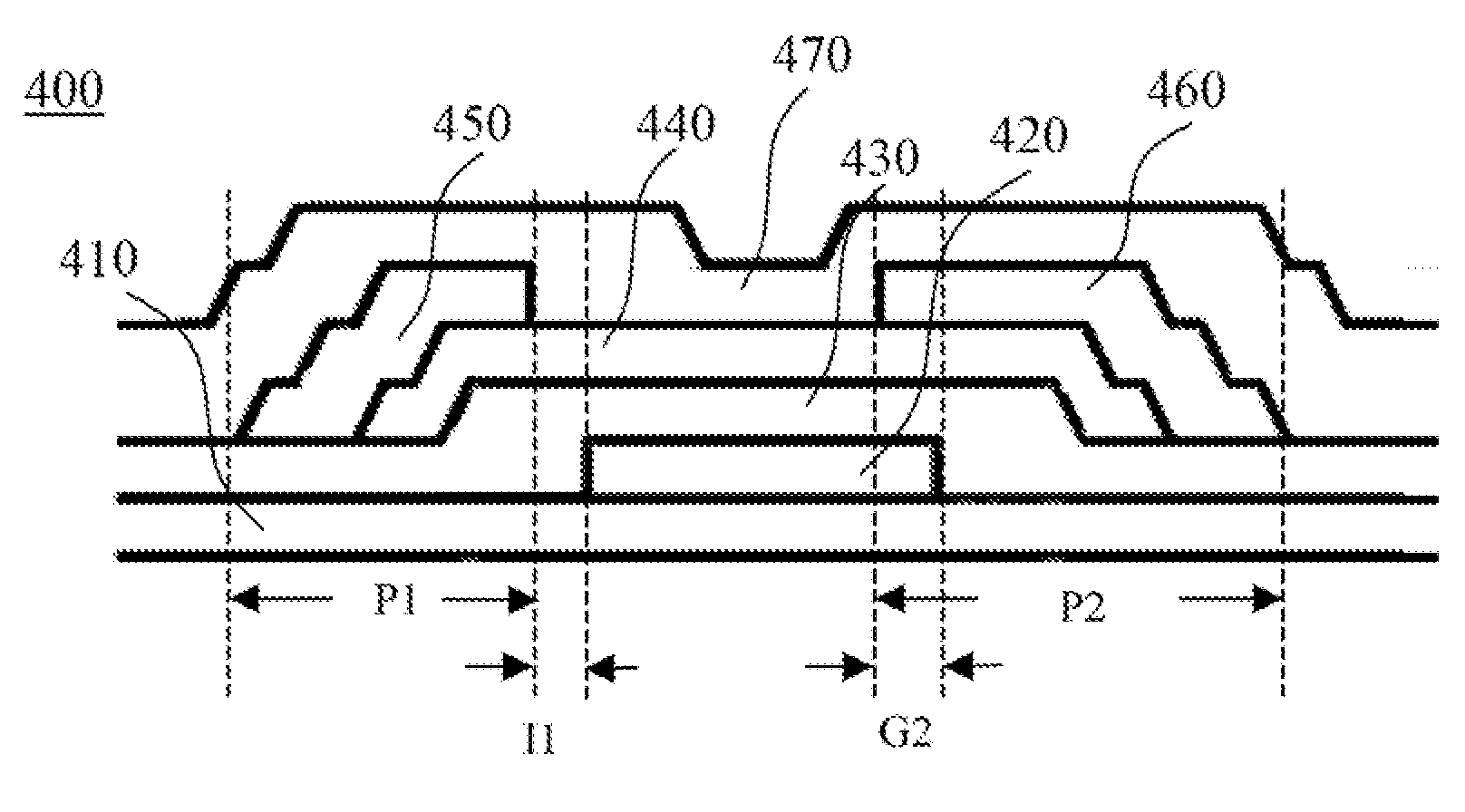
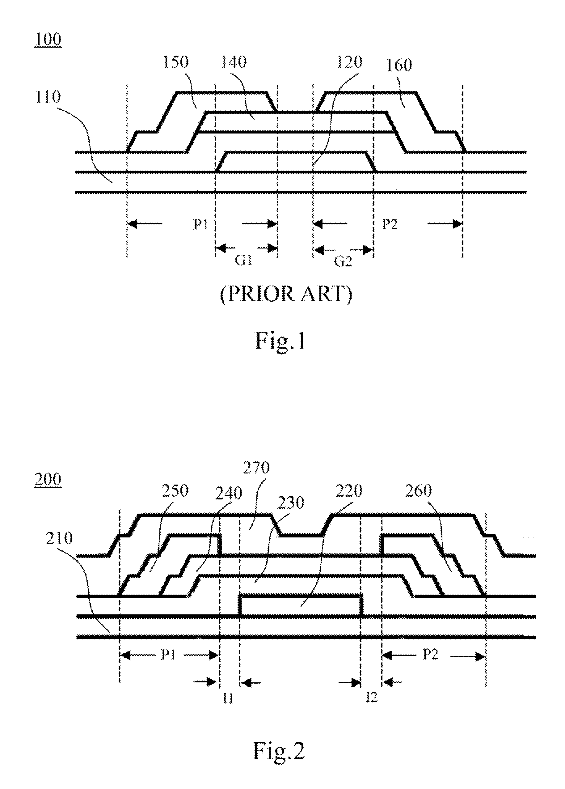
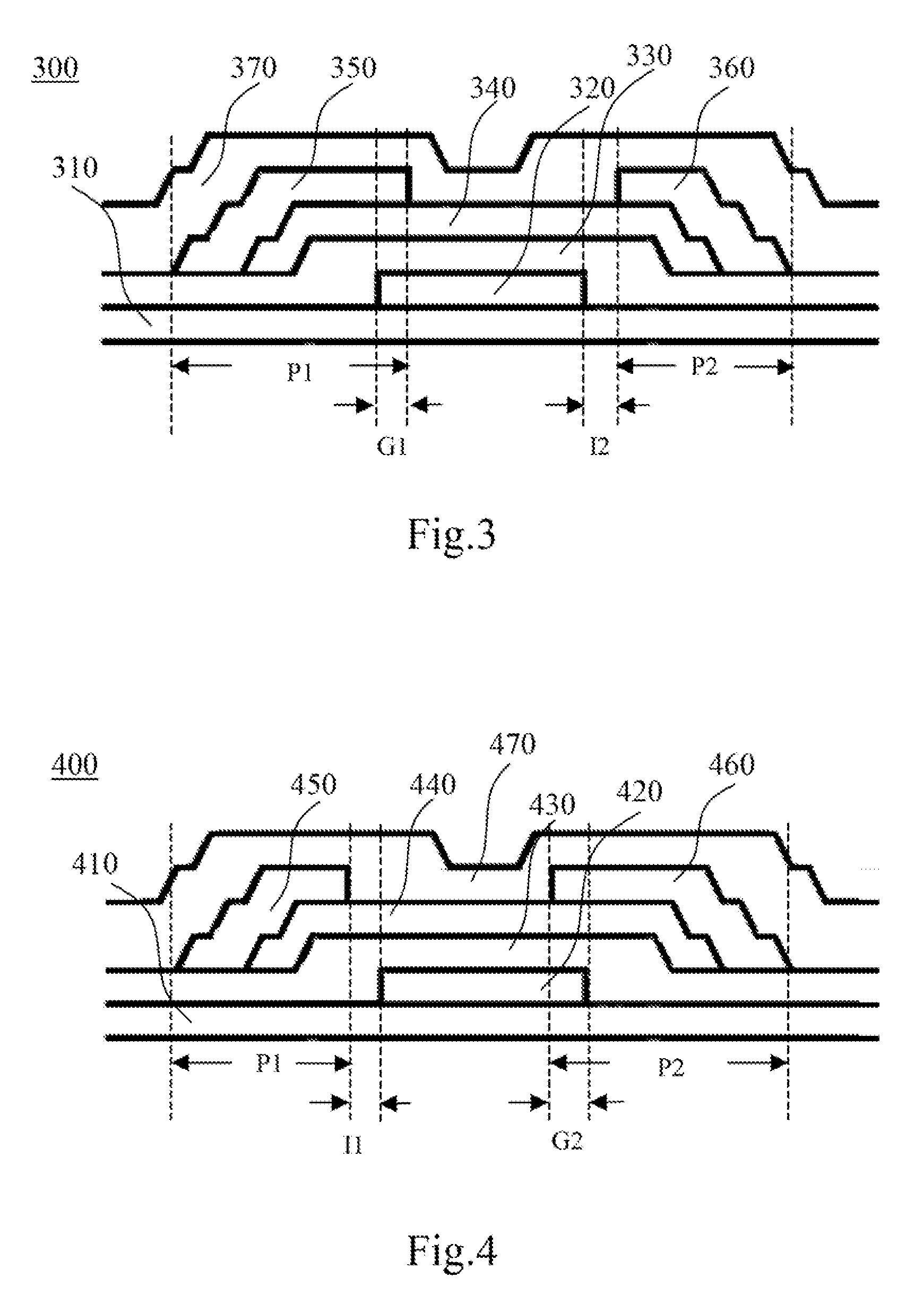
[0031]FIG. 2 is a sectional view of a metal oxide TFT 200 according to an embodiment of the present invention. The metal oxide TFT 200 includes a gate electrode 220, a gate insulating layer 230, a metal oxide active layer 240, a source electrode 250, a drain electrode 260, and an insulating layer 270. The...


PUM


Abstract

A metal oxide thin film transistor (TFT) includes a gate electrode, a gate insulating layer, a metal oxide active layer, a source electrode, and a drain electrode. The gate electrode is formed on a substrate. The gate insulating layer is formed on the substrate and covers the gate electrode. The metal oxide active layer is formed on the gate insulating layer. The drain electrode and the source electrode are formed on two opposite ends of the metal oxide active layer in a spaced-apart manner, in which at least one of the orthographic projection of the source electrode and the orthographic projection of the drain electrode on the substrate does not overlap the gate electrode.

Description

RELATED APPLICATIONS[0001]This application claims priority to U.S. Provisional Application Ser. No. 61 / 544,279 filed Oct. 7, 2011, and Taiwan Application Serial Number 101113796 filed Apr. 18, 2012, the disclosures of which are incorporated herein by reference in their entireties.BACKGROUND[0002]1. Field of Invention[0003]The present invention relates to a thin film transistor (TFT). More particularly, the present invention relates to a metal oxide TFT.[0004]2. Description of Related Art[0005]With advances in display technology and semiconductor processes, flat panel displays have been used in many kinds of electronic devices. A modern flat panel display has a thin film transistor (TFT) array substrate which is formed by a plurality of pixel units arranged in an array. Each pixel unit comprises a driving TFT and a switching TFT. The driving TFT is configured to drive a light-emitting element, and by switching on or off the switching TFT, image data can be stored in each pixel unit. ...

Claims


Application Information

Patent Timeline
Patent Type & Authority Patents(United States)
IPC IPC(8): H01L29/49H01L29/417H01L29/786
CPCH01L29/41733H01L29/7869
Inventor YEH, CHIA-CHUNWANG, HENRYTSAI, XUE-HUNGWANG, CHIH-HSUAN
Owner E INK HLDG INC
Why Eureka
Try Eureka