Successive approximation type analog-to-digital converter with variable gain and system-on-chip

An analog-to-digital converter, successive approximation technology, applied in the direction of analog/digital conversion, code conversion, signal transmission system, etc., can solve the problems of large number of components, large circuit occupation area, large power consumption, etc., and achieve small area , Increased accuracy and low power consumption

Pending Publication Date: 2021-03-30
SHANGHAI BEILING
View PDF0 Cites 0 Cited by
  • Summary
  • Abstract
  • Description
  • Claims
  • Application Information

AI Technical Summary

Problems solved by technology

[0008] The technical problem to be solved by the present invention is to provide a successive approximation analog-to-digital conversion with variable gain in order to overcome the defects of large number of components, large power consumption, and large circuit area occupied by the analog-to-digital converter in the prior art and system-on-chip

Method used


Image

  • Successive approximation type analog-to-digital converter with variable gain and system-on-chip
  • Successive approximation type analog-to-digital converter with variable gain and system-on-chip
  • Successive approximation type analog-to-digital converter with variable gain and system-on-chip

Examples


Embodiment 1

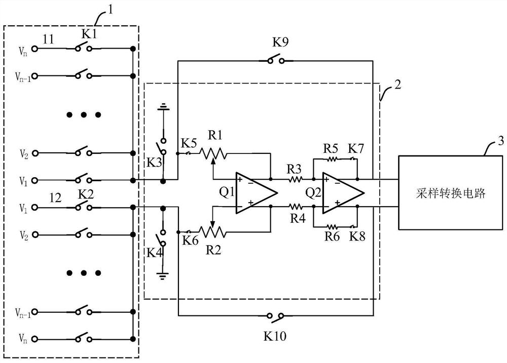
[0055] This embodiment provides a variable-gain successive approximation analog-to-digital converter. refer to figure 1 , the analog-to-digital converter includes: an input circuit 1, a variable gain amplifier 2 and a sampling conversion circuit 3.

[0056] The input circuit 1 includes multiple first input channels 11 and multiple second input channels 12, each first input channel 11 is respectively provided with a first channel switch K1, each second input channel 12 is respectively provided with a second Channel switch K2.

[0057] The output end of the first input channel 11 is connected to the first input end of the variable gain amplifier 2 , and the output end of the second input channel 12 is connected to the second input end of the variable gain amplifier 2 .

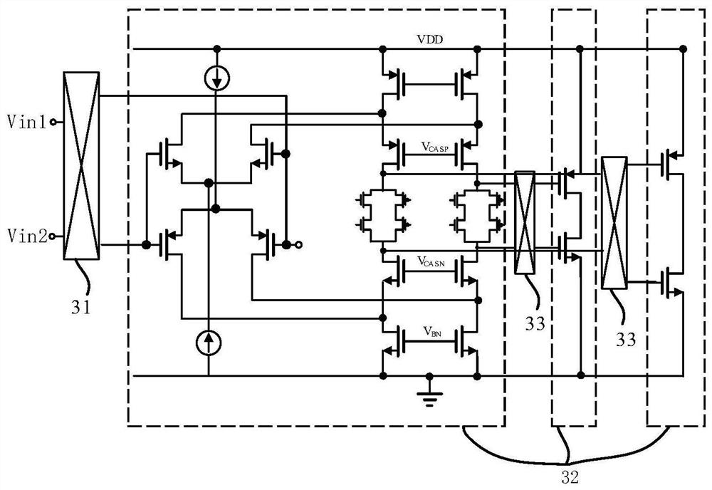
[0058] The first output terminal and the second output terminal of the variable gain amplifier 2 are respectively connected to the two input terminals of the sampling conversion circuit 3 .

[0059] The input...

Embodiment 2

[0103] This embodiment provides a system on chip, which includes the variable-gain successive approximation analog-to-digital converter described in Embodiment 1.

[0104] The system on chip of this embodiment adjusts the voltage amplitude entering the ADC through a variable gain amplifier, reduces the voltage offset and noise introduced by the variable gain amplifier through the modulation and demodulation module, increases the precision of the analog-to-digital converter, and has low power consumption , the area is small, and it can achieve fast traversal during the channel traversal process.


PUM


Abstract

The invention provides a successive approximation type analog-to-digital converter with variable gain. The successive approximation type analog-to-digital converter comprises an input circuit, a variable gain amplifier and a sampling conversion circuit, the input circuit comprises a plurality of first input channels provided with first channel switches and a plurality of second input channels provided with second channel switches. The output end of the first input channel is connected with the first input end of the amplifier, and the output end of the second input channel is connected with the second input end of the amplifier; a first output end and a second output end of the amplifier are respectively connected with two input ends of the sampling conversion circuit; the input circuit isused for inputting two paths of input signals to the amplifier by gating the first channel switch and the second channel switch; the amplifier is used for carrying out differential amplification on an input signal and outputting the signal to the sampling conversion circuit; and the sampling conversion circuit is used for sampling and analog-to-digital conversion processing of the received signals and outputting digital signals. The amplitude of the voltage entering the ADC is adjusted through the variable gain amplifier, the power consumption is low, and the area is small.

Description

technical field [0001] The invention relates to the technical field of integrated circuits, in particular to a successive approximation analog-to-digital converter with variable gain of the analog-to-digital converter and an on-chip system. Background technique [0002] With the development of integrated circuit technology, SOC (System-On-Chip, System on Chip) has been widely used. Low power consumption and small area have become the development requirements of SOC. As an important part of SOC, the analog-to-digital converter needs to convert the analog input signal to ensure the normal operation of the whole system. [0003] In the optical communication sending and receiving control MCU (Micro Controller Unit, micro control unit), it is necessary to detect a wide range of input voltages, so that in the traditional ADC (Analog to Digital Converter, analog to digital converter) multi-channel time-division sampling solution Unable to meet the requirements of the new system. ...

Claims


Application Information

Patent Timeline
Patent Type & Authority Applications(China)
IPC IPC(8): H03M1/38
CPCH03M1/38
Inventor 王冠华
Owner SHANGHAI BEILING
Why Eureka
Try Eureka