High precision optical characterization of carrier transport properties in semiconductors

a carrier transport and optical characterization technology, applied in the direction of electronic circuit testing, measurement devices, instruments, etc., can solve the problems of loss of manufacturing yield, device timing variability, and many process steps have the potential to alter or degrade the carrier transport properties, and achieve high precision optical characterization of carrier transport properties

Active Publication Date: 2021-06-03
XCALIPR CORP
View PDF0 Cites 0 Cited by
  • Summary
  • Abstract
  • Description
  • Claims
  • Application Information

AI Technical Summary

Benefits of technology

The patent describes a method for accurately measuring carrier diffusion lengths and recombination lifetimes in semiconductors using optical techniques. The method uses a parameterized function that takes into account the measurement uncertainties at each data point, the spacing of the data points, and the match of the analytic model to the data. The technique is applicable to both vacuum and laser PMR measurements. The method is particularly useful for detecting the excess carrier density in semiconductors and can provide high precision results with simple optical arrangements.

Problems solved by technology

In modern device manufacturing, many process steps have the potential to alter or degrade carrier transport properties.
Spatial and temporal shifts in process conditions cause variations in carrier transport properties, resulting in device timing variability and loss of manufacturing yield.
Although these techniques have the requisite measurement capability, they are not suitable for in-line process control due to their destructive and time consuming nature.
Such contact is disfavored in process control applications due to the attendant possibility of particulate contamination.
However, in each case some particular feature of the technique presents a significant impediment to use for in-line process control.
For example, the capacitive probes used in SPV techniques suffer from limited sensitivity (e.g. from stray capacitances) and poor spatial resolution.
The spatial resolution of SPV limits its application to “at-line” process monitoring using unpatterned blanket wafers.
Another optical technique, THz spectroscopy, is sensitive to carrier mobility but requires a complicated (and expensive) experimental setup.
Despite these advances, PMR is not widely used to determine electronic transport properties in semiconductors.
Thus in view of the appearance of the SPV in the PMR signal, the difficulties encountered in the use of SPV to determine carrier transport properties are likewise present in conventional PMR techniques.

Method used


Image

  • High precision optical characterization of carrier transport properties in semiconductors
  • High precision optical characterization of carrier transport properties in semiconductors
  • High precision optical characterization of carrier transport properties in semiconductors

Examples


Embodiment Construction

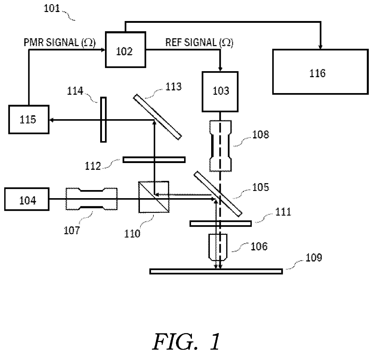
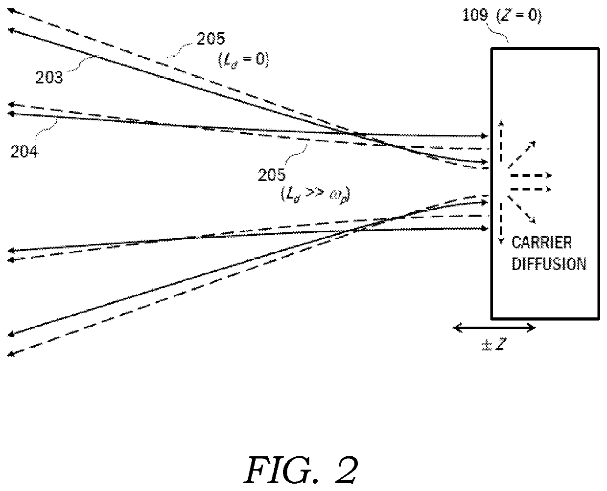
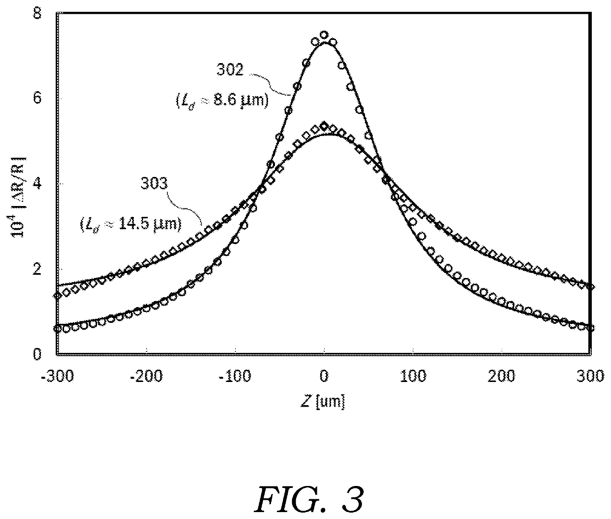
[0023]The following discusses use of the method of Z-scanning laser photo-modulated reflectance characterization of electronic transport properties in semiconductors. It is understood that the method of the present description may be used to determine electronic transport properties in any semiconductor, the discussion of exemplary silicon semiconductors considered to be exemplary only and in no way limiting in scope. It should be appreciated that the present invention provides numerous applicable inventive concepts that may be embodied in a variety of specific contexts. The specific embodiments discussed herein are merely illustrative of specific ways to make and / or use the invention and are not intended to delimit the scope of the invention.

[0024]The present invention is based upon profiling of the output signals of a laser PMR system as the sample is stepped through focus. The specific embodiments discussed here use laser beams having a cylindrically symmetric Gaussian intensity ...


PUM


Abstract

A precise optical technique for measuring electronic transport properties in semiconductors is disclosed. Using tightly focused laser beams in a photo-modulated reflectance system, the modulated reflectance signal is measured as a function of the longitudinal (Z) displacement of the sample from focus. The modulated component of the reflected probe beam is a Gaussian beam with its profile determined by the focal parameters and the complex diffusion length. The reflected probe beam is collected and input to the detector, thereby integrating over the radial profile of the beam. This results in a simple analytic expression for the Z dependence of the signal in terms of the complex diffusion length. Best fit values for the diffusion length and recombination lifetime are obtained via a nonlinear regression analysis. The output diffusion lengths and recombination lifetimes and their estimated uncertainties may then be used to evaluate various transport properties and their associated uncertainties.

Description

CROSS-REFERENCE TO RELATED PATENT APPLICATIONS[0001]The present application is a continuation and has benefit of priority of U.S. patent application Ser. No. 15 / 855,142, titled “High Precision Optical Characterization of Carrier Transport Properties in Semiconductors”, filed Dec. 27, 2017 (which is a conversion and has benefit of priority of U.S. Provisional Patent Application Ser. No. 62 / 498,685, titled “High Precision Optical Characterization of Carrier Diffusion Length, Carrier Mobility, and Sheet Resistance,” filed Jan. 5, 2017), which prior application is co-pending and has at least one same inventor of the present application and is herein incorporated by this reference.BACKGROUNDField of the Invention[0002]The present invention relates to optical measurement of electronic transport properties in semiconductors and, more particularly, to high precision measurement of carrier diffusion lengths, recombination lifetimes, diffusion coefficients, mobilities, and related carrier tra...

Claims


Application Information

Patent Timeline
Patent Type & Authority Applications(United States)
IPC IPC(8): G01R31/309G01R31/28
CPCG01R31/309G01R31/2831
Inventor CHISM, II, WILLIAM W.
Owner XCALIPR CORP
Why Eureka
Try Eureka