
Method for fabricating memory device

a memory device and fabrication method technology, applied in the field of memory devices, can solve the problems of how to design the 2t sonos memory cell, and improving the performance of the memory cell, etc., to achieve isolation capability and storage gate

Active Publication Date: 2021-07-01
UNITED MICROELECTRONICS CORP
View PDF1 Cites 0 Cited by
  • Summary
  • Abstract
  • Description
  • Claims
  • Application Information

AI Technical Summary

Benefits of technology

The invention is a memory device with a structure that improves the isolation of two gate structures. An insulating layer is used between two gate structures, and an isolation structure is formed at the top of the gate structures to provide a distance between them. This results in better performance of the memory device.

Problems solved by technology

In addition, the performance of the memory cell may get worse, while the cell sized is reduced, in which the memory cell may lose the data as store, or even cannot correctly store the data as to be stored.
How to design the 2T SONOS memory cell to improve the performed is still an issue in further development.

Method used


Image

  • Method for fabricating memory device
  • Method for fabricating memory device
  • Method for fabricating memory device

Examples


Embodiment Construction

[0032]The invention is directed to a structure of memory device and method for fabricating the memory device. The memory device may be a 2T SONOS memory device. An isolation capability between the two gate structures, such as selection gate and the storage gate may be improved. In this situation, breakdown of the memory device may be effectively reduced by improve the isolation effect at the top regions between the two gate structures.

[0033]Several embodiments are provided for describing the invention but the invention is not just limited to the embodiments as provided. Further, some of the embodiments as provided may be properly combined into another embodiment.

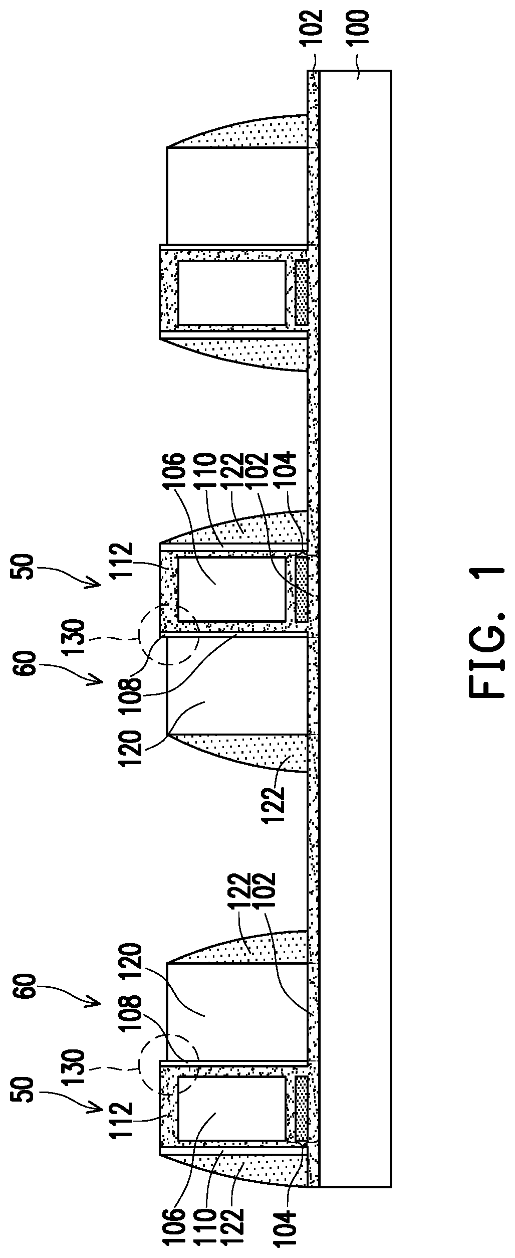
[0034]The invention has looked into the memory device with a structure of 2T SONOS memory cell and addresses at least an issue. FIG. 1 is a drawing, schematically illustrating a cross-sectional structure of a 2T SONOS memory device as to be looked into in the invention.

[0035]Referring to FIG. 1, a structure of 2T SONOS memor...


PUM

PropertyMeasurementUnit
depthaaaaaaaaaa
widthaaaaaaaaaa
non-volatile semiconductoraaaaaaaaaa

Abstract

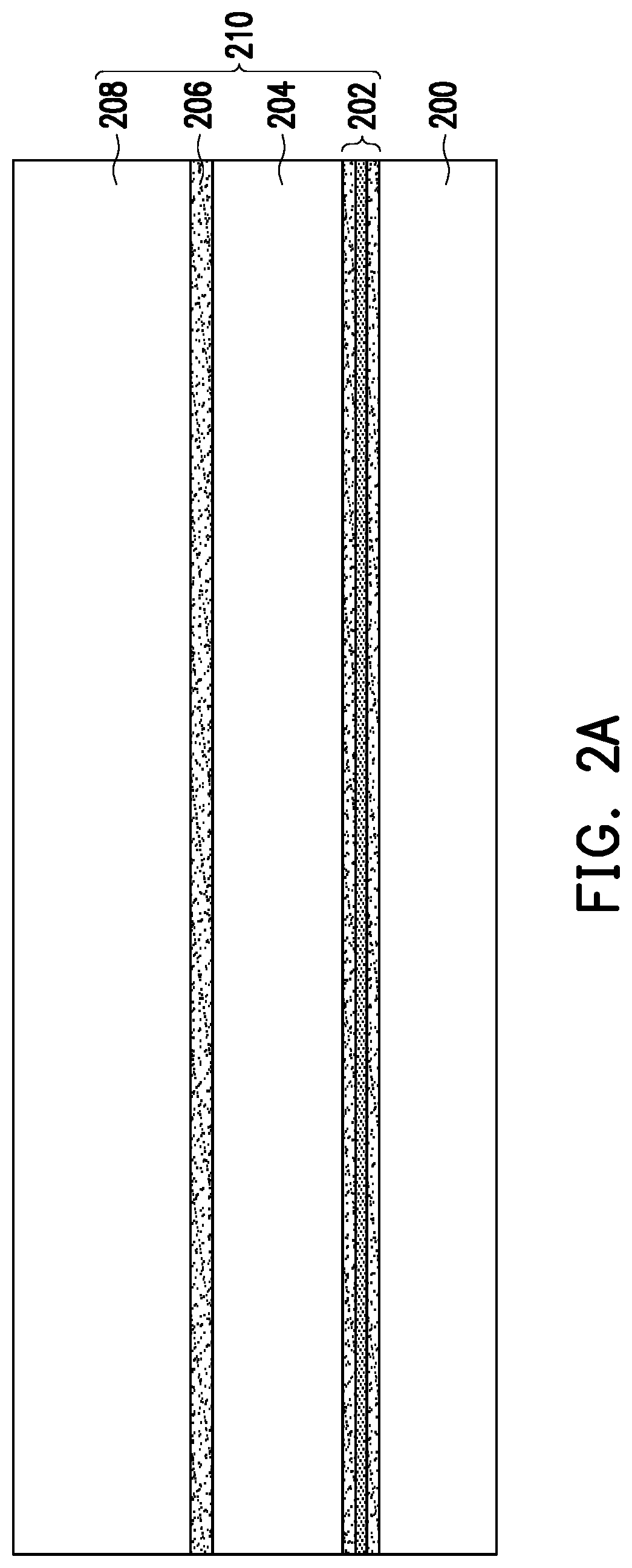
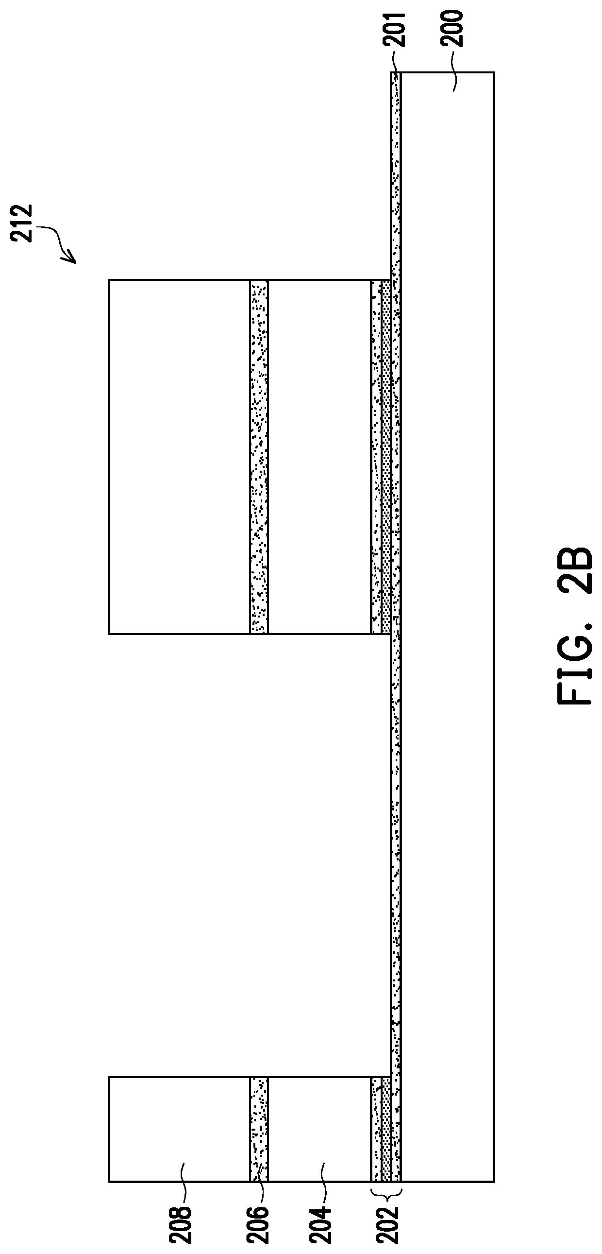
A method for fabricating memory device is provided. The method comprises forming a cell structure on a substrate, wherein the cell structure comprises a first gate structure and a second gate structure disposed on a substrate and an insulating layer in contact between the first gate structure and the second gate structure, wherein the first gate structure and the second gate structure are planarized and the first gate structure is for storing charges. Further, the first gate structure and the second gate structure are patterned to have a shallow indent above the insulating layer. An isolation structure is formed in the shallow indent to have a shallow indent isolation.

Description

CROSS-REFERENCE TO RELATED APPLICATION[0001]This application is a divisional application of and claims the priority benefit of U.S. application Ser. No. 16 / 408,214, filed on May 9, 2019, now allowed. The entirety of the above-mentioned patent application is hereby incorporated by reference herein and made a part of specification.BACKGROUND1. Field of the Invention[0002]The present invention generally relates to semiconductor fabrication, and particularly to a memory device and method for fabricating the memory device.2. Description of Related Art[0003]The non-volatile semiconductor memory has been very widely used to store data permanently as the digital information produced by various digital electronic apparatus, such as camera, video apparatus, mobile phone, flat computer, computer system, . . . , and so on. The non-volatile semiconductor memory has been a very popular tool to store a large amount of information.[0004]The digital information is produced more and more in daily lif...

Claims


Application Information

Patent Timeline
Patent Type & Authority Applications(United States)
IPC IPC(8): H01L29/423H01L29/792H01L21/02H01L21/762H01L29/66
CPCH01L29/42344H01L29/792H01L29/66833H01L21/76224H01L21/02238H01L29/40117H10B43/30
Inventor TSAI, CHIN-CHIN
Owner UNITED MICROELECTRONICS CORP
Learn More