
Semiconductor integrated circuit device
a technology of integrated circuits and semiconductors, applied in the direction of memory adressing/allocation/relocation, digital storage, instruments, etc., can solve the problems of large number of external pin terminals compared with the number of a single dram, delay in data transfer operation, and insufficient dram operation speed
- Summary
- Abstract
- Description
- Claims
- Application Information
AI Technical Summary
Benefits of technology
Problems solved by technology
Method used
Image

Examples
Embodiment Construction
of the Respective Blocks
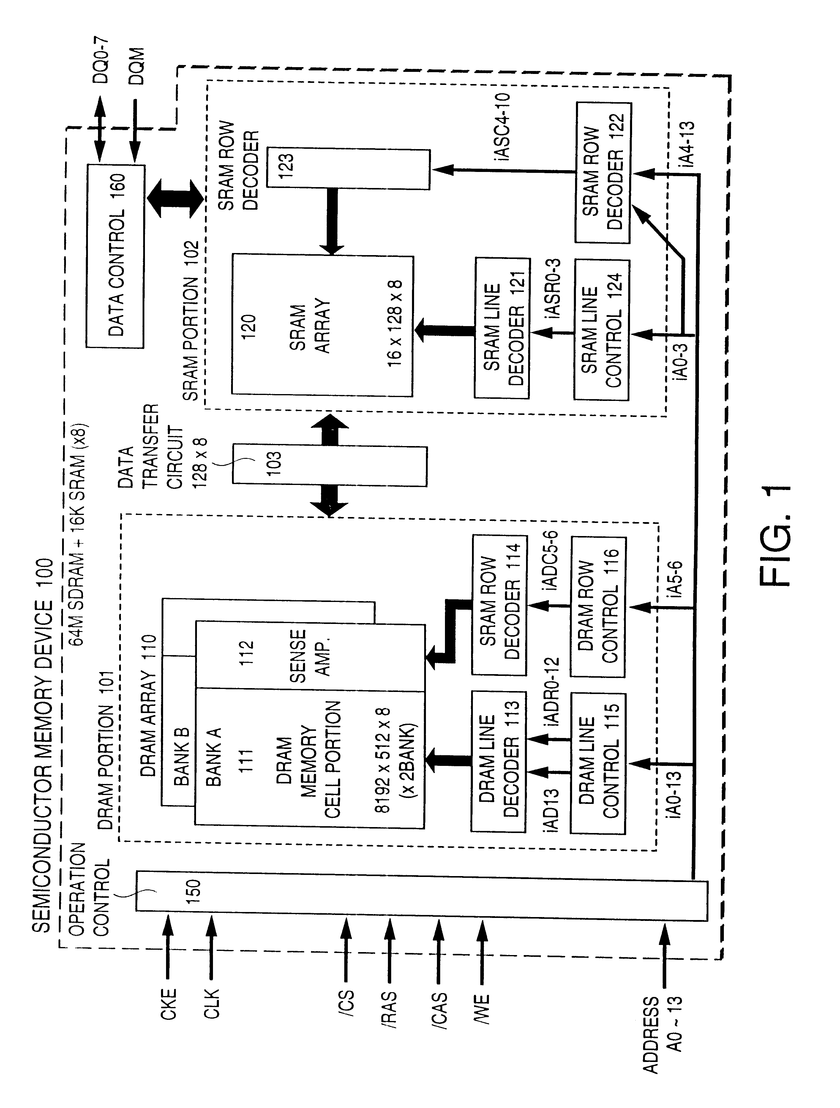
The respective circuit blocks of the overall block diagram shown in FIG. 1 will be described in detail. It should be noted that the following description is for a mere embodiment and this invention is not limited thereto.
1. {Operation Control Circuit}
FIG. 54 is a circuit diagram of the operation control circuit 150.
The operation control circuit 150 is constructed with an internal clock generator circuit 410, a command decoder 420, a control logic 430, an address control circuit 440 and a mode register 450.
The internal clock generator circuit 410 generates an internal clock signal iCLK from the external input signals CLK and CKE.
The internal clock signal ICLK is supplied to the command decoder 420, the control logic 430, the address control circuit 440 and the data control circuit to control the timing of the respective portions.
The command decoder 420 includes a buffer 421 for receiving the respective input signals and a command judge circuit 422. The / CS sig...
PUM
 Abstract
Description
Claims
Application Information