In-memory computing circuit chip based on magnetic cache and computing device
A computing circuit and magnetic technology, applied in the computer field, to achieve the effect of increasing data storage capacity, high density, and large capacity
Pending Publication Date: 2021-10-22
NANJING HOUMO TECH CO LTD
0 Cites 2 Cited by
AI-Extracted Technical Summary
Problems solved by technology
[0004] Although the reading of weight data can be avoided, the input and output...
Method used
In this implementation, a magnetic cache unit is set between two adjacent memory computing units as a data cache between the two memory computing units, and this implementation can be applied to the layer in the deep neural network during data exchange. For example, PEi processes the i-th layer of the network, PEi+1 processes the i+1-th layer of the network, and the data to be processed cached by Banki is the feature data processed by the i+1-th layer, which helps to use this circuit to cache a large amount of data And the characteristics of low power consumption can improve the performance of deep neural network.
The above-mentioned embodiment of the present disclosure provides the circuit, by setting at least one magnetic cache unit, at least one memory calculation unit, timer, using the timer to set the data retention time of the magnetic cache unit, the magnetic cache unit is in the corresponding During the data holding time, the data output by the corresponding in-memory computing unit is cached as the data to be processed, and the in-memory computing unit extracts the data to be processed for calculation, and outputs the calculated data to other magnetic cache units. Therefore, the characteristics of higher density and larger capacity of the magnetic cache unit compared with the static random access memory are effectively utilized, and the data storage capacity inside the chip when performing in-memory calculations is improved. In addition, since the data retention time is set for the magnetic cache unit, and the data retention time can be set according to the data processing capacity of the computing unit in the memory, it can overcome the defect of high write power consumption due to the long write delay of the magnetic cache unit , effectively utilizing the characteristics of short write delay and low write power consumption of the magnetic cache unit, flexibly adjust the data retention time of the magnetic cache unit in various in-memory computing scenarios, and realize...
Abstract
The embodiment of the invention discloses an in-memory computing circuit based on a magnetic cache, and the circuit comprises at least one magnetic cache unit, at least one in-memory computing unit, and a timer. The magnetic cache unit in the at least one magnetic cache unit is used for caching data output by the corresponding in-memory computing unit as to-be-processed data within the corresponding data retention time; the timer is used for respectively setting data retention time for the at least one magnetic cache unit; and the in-memory computing unit in the at least one in-memory computing unit is used for extracting the data to be processed from the corresponding magnetic cache unit for calculation and outputting the computed data to other magnetic cache units. According to the embodiment of the invention, the invention achieves the flexible adjustment of the data retention time of the magnetic cache unit in various in-memory calculation scenes, and achieves the provision of a high-capacity cache for the data needed by in-memory computing under the lower power consumption.
Application Domain
Digital storageNeural architectures +1
Technology Topic
Data needsEngineering +5
Image
Examples
- Experimental program(1)
Example Embodiment
[0028] Next, an exemplary embodiment according to the present disclosure will be described in detail with reference to the accompanying drawings. Obviously, the described embodiments are merely a part of the embodiments of the present disclosure, not that the embodiments of the present disclosure, to be understood, and the present disclosure is not limited by the example embodiments described herein.
[0029] It should be noted that the relative arrangement of the components and steps set forth in these embodiments, unless otherwise specified, the digital expression and the numerical value are not limited to the scope of the disclosure.
[0030] Those skilled in the art will appreciate that "first", "second" in the present disclosure is only used to distinguish different steps, devices or modules, etc., neither represent any particular technical meanings, nor Inevitable logic order.
[0031] It should also be understood that in the present disclosure embodiment, "multiple" may refer to two or more, "at least one" can refer to one, two or more.
[0032] It should also be understood that any of the components, data, or structures mentioned in the embodiments of the present disclosure may be generally understood to be one or more in the case where there is no explicit defined or reverse inspiration in the foregoing.
[0033]Further, the present disclosure "and / or" is merely a relationship of the associated object, indicating that there may be three relationships, such as A and / or B, which can be represented: Alone present A, while there is A and B There are three cases of B alone. Further, the characters "/" in the present disclosure generally indicate the relationship between the front and rear associated objects is a "or".
[0034] It will also be understood that the present disclosure emphasizes the differences between the various embodiments, which may be referenced in the same or similarities, for simple, no longer
[0035] At the same time, it should be understood that in order to facilitate the description, the dimensions of the respective portions shown in the drawings are not drawn in accordance with the actual ratio relationship.
[0036] The following description of at least one exemplary embodiment is actually illustrative only, and it is not necessary to use any limits to the present disclosure and its application or use.
[0037] For technical, methods, and equipment known to those of ordinary skill in the art may not be discussed in detail, in appropriate, the techniques, methods, and equipment should be considered part of the specification.
[0038] It should be noted that similar reference numerals and letters represent the like items in the drawings below, and therefore, once a certain term is defined in one drawing, it is not necessary to discuss it in the following drawings.
[0039] Application overview
[0040] The cache of the existing depth learning storage architecture is typically designed based on SRAM (static random access memory, staticrandom-access memory) device device. Based on SRAM's cache, it is difficult to cache all activated feature data due to the lower SRAM density, and it is difficult to cache all activated feature data. On the other hand, since the static power consumption of SRAM is large, it will affect the overall calculation architecture in the memory. efficiency.
[0041] MRAM (Magnetic Random Memory, MagnetoreSistive Random Access Memory) can be used to construct a non-volatile memory unit in the stored computing architecture, using its longer hold time to store weight data. The MRAM in the existing store calculation architecture is mainly used to store weights with its non-volatile characteristics. Overall energy efficiency.
[0042] The existing mainstream MRAM is multi-rotating moment mode writes data, and its write mode is the current pass-through magnetic tunnel junction (MTJ) change the free layer state in the MTJ. Generally, the memory needs to meet thermal stability to meet the requirements of non-lost memory, and its storage data can be expressed as:
[0043]
[0044] During δ represents thermal stability, when it is greater than 60, the MRAM memory data can be maintained for more than 10 years.
[0045]
[0046] Where V represents the voltage value, h k Indicates magnetic anisotropy, M s Indicates that saturation magnetization strength, T represents temperature. For MTJ writing critical current, it is with current density J c0 And the relationship between writing time is shown in the formula:
[0047]
[0048] Although different MRAM design, the above parameters are slightly unused, but they all obey a law: the write delay is long, the write power consumption is high, the data is maintained long; in turn, the write delay is short, the write power is low, Then the data holds short.
[0049] Table 1 provides a comparison of various parameters of different scenarios (Note: Different MRAM design corresponds to different data).
[0050] Table 1 mRam different holding time corresponding to write time and write energy example (CLK = 1ns)
[0051] Case1 Case2 Case3 Case4 Case5 Case6 T retention
[0052] According to the write delay, power consumption, holding time of the magnetic storage device given in Table 1, the present disclosure provides an MRAM cache that supports "multi-hold time", ie magnetic buffer units under different use scenarios, Set different data hold time.
[0053] Exemplary structure
[0054] figure 1 It is a schematic structural diagram of a magnetic buffer-based memory computing circuit provided by an exemplary embodiment of the present disclosure. The respective components contained in the circuit can be integrated into one chip, or may be set to a different chip or circuit board, and a link between the data communication between these chips or boards can be established.
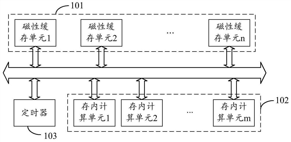
[0055] like figure 1 As shown, the circuit includes: at least one magnetic buffer unit 101 (including magnetic buffer unit 1-magnetic buffer unit N), at least one memory computing unit 102 (including in-memory computing unit 1-memory computing unit M), Timer 103. The above at least one magnetic buffer unit 101, at least one in-memory computing unit 102 and the timer 103 can be connected via a bus 104.
[0056] In the present embodiment, the magnetic buffer unit in the at least one magnetic buffer unit 101 is used to cache data outputted by the corresponding memory computing unit within the corresponding data hold time as the data to be processed. For example, when the circuit is applied to the data operation of the depth neural network, each of the magnetic buffer units in the at least one magnetic buffer unit 101 can be used to cache feature data of a convolution layer, and the feature data of the cache is usually. The data outputted is calculated for the corresponding storage computing unit. The magnetic buffer unit may be a memory cell constructed by the above MRAM, typically, a magnetic buffer unit can be referred to as a MRAM BANK. Magnetic storage arrays, data read / write interfaces, and other modules can be included in each magnetic buffer unit.
[0057] In the present embodiment, the timer 103 is used to set the data hold time for at least one magnetic buffer unit 101.
[0058] Among them, for the magnetic buffer unit in at least one magnetic buffer unit, the data hold time corresponding to the magnetic buffer unit is predetermined based in first, the data amount of the tortured data processed by the magnetic buffer unit, and the magnetic buffer unit corresponds. The in-depth calculation unit is obtained.
[0059] As an example, a magnetic buffer unit may correspond to a memory computing unit, and the magnetic buffer unit stores a certain amount of data to be processed, and the data to be processed is data outputted in the corresponding memory computing unit. Generally, the amount of data to be processed to be processed is divided by the power throughput of the in-memory computing unit (i.e., the amount of the data of the unit time processed), the resulting calculation result is the time required to process the data in the store. At the same time, this time is the shortest time for the magnetic buffer unit to maintain these to process data stably stored in it.
[0060] Optionally, the above calculation results can be determined as the data hold time corresponding to the magnetic buffer unit. It is also possible to find the data hold time corresponding to the calculation result as the data hold time of the calculation result as the data hold time of the calculation result as the data hold time of the calculation result as the data hold time of the calculation result as the data hold time that is closest to the calculation result is obtained from the pre-established method (e.g., the above table 1). .
[0061] Timer 103 can be implemented in a variety of ways, such as real time clock, crystal radioscopy, and the like.
[0062] The memory computing unit in the at least one memory computing unit 102 is used to extract the data to be processed from the corresponding magnetic buffer unit, and output the calculated data to other magnetic buffer units. Typically, one memory computing unit may correspond to at least two magnetic buffers, one for storing the tortoise data required to store the memory computing unit, and other magnetic cache units are used to cache data outputted by the memory computing unit as other departments. The data of the inner calculation unit is processed. Alternatively, a magnetic buffer unit can correspond to at least two memory computing units, one for outputting data to the magnetic buffer unit as other indi-computing units to be processed.
[0063] It should be noted that the inline computing unit may be an in-depth computing unit of any arbitrary architecture, and the embodiments of the present disclosure will not be described again regarding the implementation of the interior computing unit. In the present embodiment, the number of in-memory computing units included in the at least one memory computing unit 102 can be equal to the number of magnetic cache units included in the at least one magnetic buffer unit 101, or may be equal, ie figure 1 The number of magnetic buffers in the magnetic buffer unit may be the same as the number M of the inner computing unit, or may be different.
[0064] The circuit provided by the above embodiment provided by the present disclosure, by providing at least one magnetic buffer unit, at least one memory computing unit, the timer, using the timer to set the data hold time of the magnetic buffer unit, the magnetic buffer unit holds time at the corresponding data Inside, the data output by the cache corresponds to the data to be processed, and the memory computing unit extracts the calculation of the data to be processed, and outputs the calculated data to other magnetic cache units. Thus, the magnetic buffer unit is utilized to increase the data storage amount inside the chip during memory computing when the magnetic buffer unit is higher and more capacity. Further, since the magnetic buffer unit sets the data hold time, and the data hold time can be set according to the amount calculation unit data processing amount, it can overcome the defective defects that write power consumption of the magnetic buffer unit write delay. , Effectively use the magnetic buffer unit write delay short writing power, flexibly adjust the data hold time of the magnetic buffer unit under various storage, realization of lower power consumption, computing The data required provides higher capacity cache.
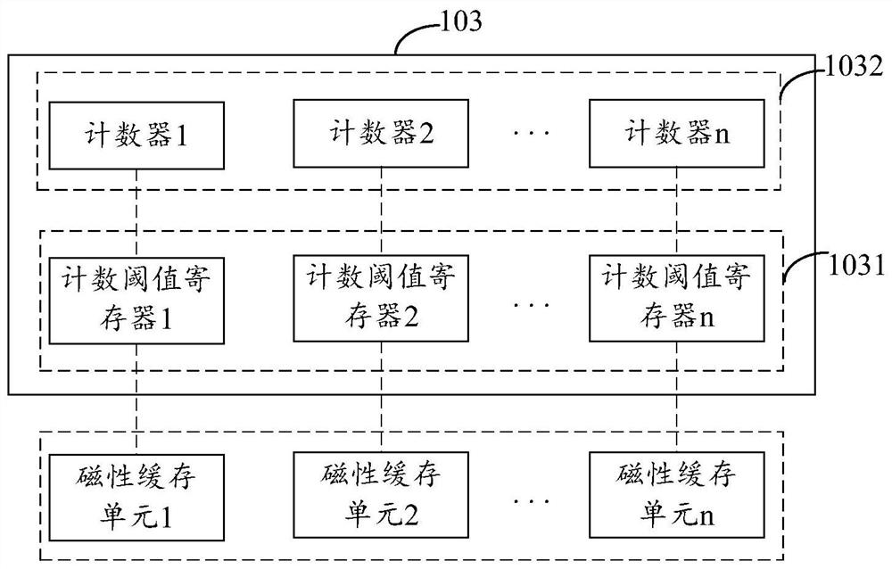
[0065] In some optional implementations, such as figure 2 As shown, the timer 103 includes at least one count threshold register 1031 and at least one counter 1032, at least one counter 1032, at least one count threshold register 1031, at least one magnetic buffer unit 103 corresponds to one by one. like figure 2 The counter 1, the counting threshold register 1, the magnetic buffer unit 1 corresponds to the counter 2, the counting threshold register 2, and the magnetic buffer unit 2 correspond to; ...; counter N, count threshold register N, magnetic buffer unit N corresponds .
[0066] For the count threshold register in at least one count threshold register 1031, the counting threshold register is used to store a pre-set count threshold, and the count value of the counter corresponding to the count threshold register is of the time the count threshold passed by the initial count value to the count threshold. The data hold time of the magnetic buffer unit corresponding to the unit.
[0067] As an example, a count threshold register is stored in a count threshold having a counting period of 1 ns. The initial count value is 0, the count value is counted from 0 to 4, and after 4 count cycles (ie 4ns), count The value of zero, that is, the data hold time of the magnetic buffer unit corresponding to the counter corresponding to the counter is 4ns.
[0068] It should be noted that the circuit units described in the present application embodiment are merely schematic, and the specific structures are not limited. The respective units included in this circuit can be any combination. For example, the above count threshold register may be disposed in a circuit region separate from each of the magnetic buffer units and respective deposit computing units, and the respective counters may be set to the same circuit region with respective magnetic buffer units, respectively.
[0069]In this implementation, the timer implemented by the counter and the count threshold register, when the corresponding memory computing unit performs data processing, it is not necessary to accurately perform the timing of the data hold time, only set the count threshold, thereby reducing the data remaining Time to make a timing, help to improve the efficiency of in-memory computing.
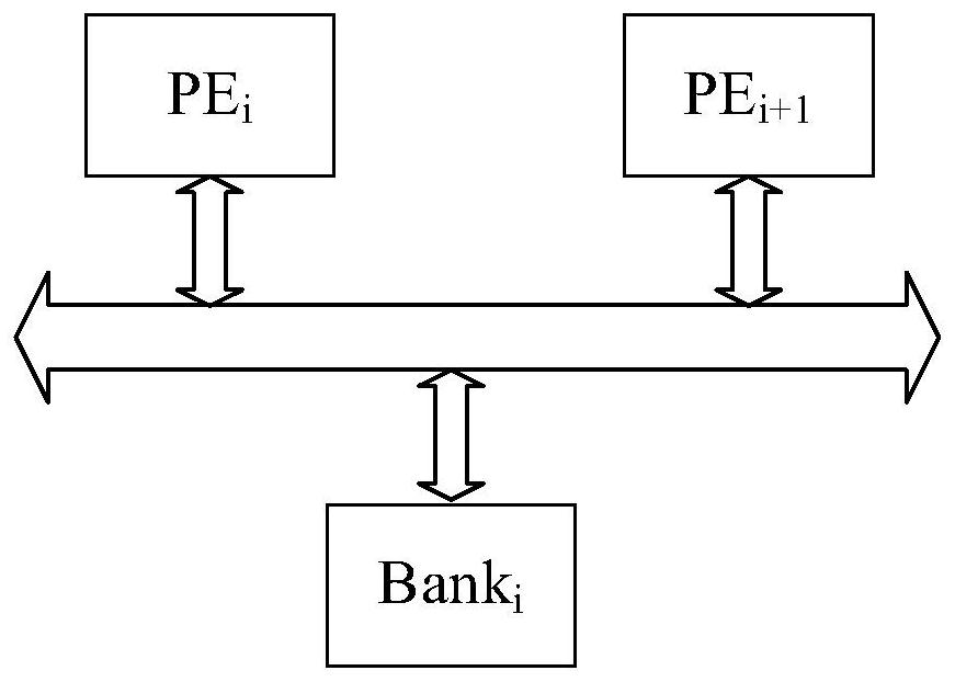
[0070] In some alternative implementations, for the magnetic buffer unit in at least one magnetic buffer unit, the magnetic buffer unit corresponds to one of at least one in-depth computing unit and one in the rear depository calculation unit. The magnetic buffer unit is configured to store data to be processed in the first stored data, and after the respective data hold time is used, the data is processed from the magnetic buffer unit and the processing data is processed. calculate.
[0071] like image 3 As shown in the i-th memory calculation unit PE i , 1 + 1 memory calculation unit PE i+1 And i-th magnetic buffer unit Bank i Connect to the bus. Where PE i Bank i In the first store calculation unit, PE i+1 Bank i In the rear depository calculation unit. PE i The output data is stored as the data to be stored to Bank i Medium, PE i+1 After the corresponding data holds time, from Bank i A certain amount of to be processed is extracted in the calculation. Optional, Bank i The storage data stored in the store can be PE i The full amount of data is output, or it can be PE i Some data output.
[0072] This implementation sets a magnetic buffer unit between the two adjacent memory computing units as a data cache between the two memory computing units, which can apply this implementation to inter-neural data exchange. During the process. , For example, PE i Handling the i-level of the network, PE i+1 Handling i + 1 floor of the network, Bank i The buffered data is characteristic data for the i + 1 layer processing, thereby helping the use of the circuit cache volume and smaller power consumption, and improve the performance of the depth neural network.
[0073] In some alternative implementations, for the magnetic buffer unit in at least one magnetic buffer unit, the magnetic buffer unit is used to store partial data outputted in the first-store internal computing unit as the data to be processed, wherein the magnetic buffer unit corresponds to The data hold time is based on the number of data outputted in the first-stored computing unit and determines the amount of data required to calculate the calculation unit in the post-memory computing unit in the post-memory computing unit. In the present implementation, after the pending data stored in a magnetic buffer unit reaches a certain amount, the corresponding calculation unit can be calculated from the magnetic buffer unit, that is, the pipeline type is realized. data processing.
[0074] As an example, such as Figure 4 Disted, h i+1 The height of the Feature Map calculated for the first + 1 layer of the depth neural network, K i+1 Size, CH, CH, CH, CH, CH i+1 Indicates the number of channels of Feature Map calculated by the first layer. When the above Bank i The inner cache is to be processed Like Figure 4 The number of data filled in Feature Map), the above PE i+1 You can start the data calculation. When this calculation is completed, the volume core moves, the i-th layer outputs the new to-process data and caches the above Bank. i Thus, the inter-neural network of inter-neural network is realized.
[0075] In this implementation method, Bank i Data hold time t retention It can be expressed as:
[0076]
[0077] Among them, Throughput i For the above PE i The interactive throughput rate. Typically, for most depth neural networks, T retention <25 μs, therefore, it is usually selected that the case1 in Table 1, that is, the count threshold value of the i-th count threshold register is set to 4.
[0078] The flow wire-based data processing method provided in this realization is compared to the full amount of data output by the magnetic buffer unit, and can be processed by the bundled part calculation unit after the cache part is processed. The requirements for the volume of the magnetic buffer unit are reduced to help reduce the cost and implementation of the circuit. Further, since the number of internal computing unit processing data is reduced, the data hold time of the corresponding magnetic buffer unit can be reduced accordingly, and the power consumption of the magnetic buffer unit can be further reduced.
[0079] In some alternative implementations, for the magnetic buffer unit in at least one magnetic buffer unit, the magnetic buffer unit is configured to store all of the data outputted by the first store as the data to be processed. The data hold time corresponding to the magnetic buffer unit is based on the number of data outputted in the first-store, and determined in the interactive power throughput of the calculation unit in the first store.
[0080] As an example, such as Figure 5 Disted, h i+1 And W i+1 The height and width of FeatureMap calculated by the Deep Neural Network, respectively, CH i+1 Indicates the number of channels of Feature Map calculated by the first layer. Bank i The inner cache is processed (like Figure 5 The number of all data in Feature Map), the above PE i+1 Extract the full amount of data outputted by the i-layer to perform data processing of the interlayer shared (non-flow) mode of the depth neural network.
[0081] In this implementation method, Bank i Data hold time t retention It can be expressed as:
[0082]
[0083] Among them, Throughput i For the above PE i The interactive throughput rate. Typically, for most depth neural networks, when using this implementation, the count threshold of the first count threshold register is typically selected to 4.
[0084] The present implementation passes the full amount of data outputted in the first-store calculation unit by the magnetic buffer unit, further enriches the data buffer mode in the in-memory computing process, and the scope of the application scenario applies to the circuit is expanded, compared to the above-described water. The pattern of data processing is small, and the probability of timing errors that occur when the cache is to be processed, thereby helping to improve the calculation accuracy of the in-memory computing circuit.
[0085] In some alternative implementations, for the magnetic buffer unit in at least one magnetic buffer unit, the magnetic buffer unit corresponds to one of at least one in-memory computing unit in the first-stored internal computing unit and the predetermined number in the latter. Internal computing unit, the magnetic buffer unit is used to store data to be output in the first-lamination computing unit and the preset number of data respectively output as the data to be processed, wherein the data hold time corresponding to the magnetic buffer unit is based on the pre- The number of the number of pending data corresponding to the respective calculation units respectively corresponds to the rear depository calculation unit.
[0086] Wherein, the preset number is respectively corresponding to the in-depth computing unit, that is, the data output by each of the previous memory computing units adjacent to the rear deposit. The above target storage computing unit is typically the last one of the above predetermined number of computing units in the rear deposit.
[0087] like Image 6 As shown in the i-th memory calculation unit PE i , 1 + 1 memory calculation unit PE i+1 , ..., i + L memory calculation unit PE i+l And i-th magnetic buffer unit Bank i Connect to the bus. Where PE i Bank i In the first store calculation unit, PE i+1 , ..., PE i+l Bank i In the rear depository calculation unit. PE i PE i+1 , ..., PE i+l The output data is to be processed, where PE i+l Due to the need for PE i The output to be processed is calculated, so PE i The output of the output needs to be processed to PE i+l When the corresponding peer data is output, ie at PE i+l After outputting the data to be processed, PE i Output to be processed by other computing modules from Bank i Extract and process it. Optional, in this implementation, Bank i The pending data stored in the stored data may be full data output in each in-depth computing unit (as described above) Figure 5 The scheme corresponding to the embodiments may be part of the data output, such as the above Figure 4 The scheme described in accordance with the embodiment).
[0088] In this implementation method, Bank i Data hold time t retention It can be expressed as:
[0089]
[0090] Among them, Throughput j Corresponding PE j The interactive throughput rate. Got T retention Once, the corresponding data hold time can be found based on the table one.
[0091] As an example, such as Figure 7A As shown, for the RESNET network, the Feature Map output for a convolution layer can be used across two layers, ie Figure 7A The FEATURE MAP output in the i-layer output will be used after the i + 2 layer is processed again. Under the application scenario, the data hold time of the magnetic buffer unit typically selects CASE2 or CASE3 in Table 1. like Figure 7b As shown, the Feature Map outputted by the detection task is used for the Feature Map output for a convolution layer, which will be used across multiple layers. Figure 7b The FEATURE MAP output from the i-layer is used after the data of the i + 4 layer is used, and the application scenario is used, the data hold time of the magnetic buffer unit usually selects Case5 or even Case6 in Table 1. Sufficient hold time.
[0092] The present implementation ensures that the data output by the magnetic buffer unit in the pre-deposit computing unit is completed in the post-memory cell processing data, so that the circuit can be applied to a neural network such as RESNET, FPN. Further enriching the data cache mode during the storage process, the scope of the application scenario applicable to the circuit is expanded.
[0093] In some optional implementations, for the magnetic buffer unit in at least one magnetic buffer unit, the data hold time corresponding to the magnetic buffer unit is less than the conservative data hold time corresponding to the pre-established magnetic buffer unit.
[0094] Among them, the conservative data hold time is determined according to the amount of data, the minimum hold time when writing data is written. As an example, the second line of the above table (T w The corresponding time is the conservative data hold time. When the duration of the data is written to reach a conservative data hold time, the magnetic cache can be guaranteed to achieve the expected higher reliability. Typically, after the data amount and the power throughput of the tortoise data processing based on the in-depth computing unit are properly shortened, the data hold time can be properly shortened, and the shortened time can be arbitrarily set.
[0095] Typically, when an actual data hold time is set, it is determined based on the distribution of the write failure when writing data to the magnetic buffer unit. For example, the correspondence between writing failure and data hold time is like Figure 8 As shown, the distribution curve is obtained by the following formula:
[0096]
[0097] Where P usw Indicates that there is no probability density of the flip (ie, writing failed), τ represents the current load time, δ represents the structuring thermodynamic stability parameters of the magnetic buffer unit, i C Represents a critical current value. like Figure 8 As shown, when it is determined that the magnetic buffer unit complies with the case3 in the table, the conservative data hold time is 4.38 ns, and the actual data hold time can be set to 4ns, thereby estimating that 5% of the data cannot reach sufficient holding. time.
[0098] The present implementation can reduce the power consumption of the magnetic buffer unit by setting the actual data hold time of the magnetic buffer unit to be less than the conservative data hold time, can reduce the power consumption of the magnetic buffer unit in the case where the probability of writing the magnetic buffer unit is in the range of tolerance. Improve data write speed.
[0099] In some alternative implementations, the magnetic buffer units in the at least one magnetic buffer unit include a reliable area and a unreliable area, a reliable area for storing important data, unreliable data for storing non-important data.
[0100] Among them, the reliable area and unreliable area of the magnetic buffer unit can be defined by the aging test method of the existing storage device. For example, sub-units of each storage bit in the magnetic buffer unit perform data write operation according to the target write time, and this operation can be repeated several times, and then read the data, determine the sub-unit written in accordance with the read result according to the read result. Then divide the reliability area and the unreliable area.
[0101] The above important data and non-important data can be set in a variety of ways. Please refer to the following optional implementations.
[0102] This implementation is stored in a non-reliable area by setting a reliable region and an unreliable area in the magnetic buffer unit, and the important data is stored in a reliable area, and the non-important data is stored in an unreliable area, thereby achieving a magnetic buffer unit due to shortening data hold time. In the case where the write error rate is improved, the probability of writing an error occurring as much as possible is reduced, and the reliability of the data cache is improved on the basis of reducing the power consumption of the magnetic buffer unit.
[0103] In some optional implementations, important data includes the following: Data on the high bit bit of the multi-bit data including the preset bits, based on the important data determined by the pre-performed data importance; Important data includes the following: Data on a low bit in a low bit in the high bit of preset bits in the multi-bit data, based on important data determined based on importance division.
[0104] Specifically, the above predetermined position can be determined based on the ratio of the total capacity of the magnetic buffer unit in the unreliable region. For example, if the unreliable area accounts for the total capacity ratio <25%, for the 8-bit data, the high 6-bit is stored in the reliability area, and the low 2-bit is stored in a unreliable area. Thereby, the reliable region is stored in a high bit, and the magnitude of the change in data is changed.
[0105] The above data importance division method can be used in existing methods. For example, when the circuit is applied to the field of depth neural network, an existing analytical method for algorithmic interpretability can be employed to determine the importance of data contained in each channel in the neural network.
[0106] This implementation provides a partitioning scheme for non-important data, which enables data to be stored in the magnetic buffer unit to deposit into different regions in the magnetic buffer unit, thereby helping to reduce the circuit. The probability of calculating the error occurred during internal calculation.
[0107] Embodiments of the present disclosure also provide a chip that integrates a magnetic buffer-based memory computing circuit, a magnetic cache based memory computing circuit, such as Figure 1 - Figure 8 And related descriptions, this is not disclosed herein.
[0108] The embodiment of the present disclosure also provides a computing device including the chip described above. Further, the computing device may further include an input device, an output device, and a necessary memory, or the like. The input device can include, for example, a mouse, a keyboard, a touch screen, a communication network connector, or the like for inputting the original array. The output device may include data such as a display, a printer, and a communication network, and a connected remote output device, or the like, for outputting data of the second preset representation described above described above. The memory is configured to store data input by the above input device, and data generated during the operation of the magnetic cache is calculated. Memory can include volatile memory and / or non-volatile memory. Volatile memory, for example, can include a random access memory (RAM) and / or a cache, and the like. Non-volatile memory, for example, can include read only memory (ROM), hard disk, flash memory, and the like.
[0109] The above combined with the specific embodiments describe the basic principles of the present disclosure, but it is necessary to indicate that the advantages, advantages, effects, etc. mentioned in the present disclosure are only example rather than limitations, and these advantages, advantages, effects, etc. are not considered. The various embodiments of the present disclosure must have. Further, the specific details of the above disclosure are merely for example and to facilitate understanding, but not limitation, the details are not limited to the present disclosure, which must be implemented in the above specific details.
[0110] The various embodiments in this specification are described in the manner, each of which is the same as that of other embodiments, and the same or similar parts of each of the embodiments can be referred to.
[0111] The block diagrams of the device, apparatus, device, and system according to the present disclosure are only examples of exemplary examples and are not intended to require or imply, and must be connected, arranged, and configured in a manner shown in block diagram. As will be recognized, these devices, devices, devices, and systems can be configured in any manner. Words such as "including", "include", "" ", etc., are open vocabulary, refers to" including but not limited to ", and can be used interchangeably. The vocabulary "or" and "referred to herein" and / or ", and can be used interchangeably, unless the context explicitly indicates that is not. The vocabulary used herein ", such as" refer to ", such as, but not limited to", and can be used interchangeably.
[0112] The circuit of the present disclosure may be implemented in many ways. For example, the circuit can be implemented by software, hardware, firmware, or software, hardware, and firmware any combination of the present disclosure. The above sequence of the steps of the method used in the circuit is merely illustrative, and the steps of the methods of the present disclosure are not limited to the above specific description, unless otherwise specifically described. Further, in some embodiments, the present disclosure may be implemented as a program recorded in a recording medium, which includes a machine readable instruction for implementing the function of the circuit according to the present disclosure. Therefore, the present disclosure also covers a recording medium stored in a program for performing the function of the circuit according to the present disclosure.
[0113] It is also noted that in the circuit of the present disclosure, each component or each step is to decompose and / or recombine. These decomposition and / or recombination should be considered as an equivalent solution of the present disclosure.
[0114] The above description of the disclosed aspects is provided to enable any skilled in the art to make or use the present disclosure. Various modifications to these aspects will be apparent to those skilled in the art, and the general principles defined herein can be applied to other aspects without departing from the scope of the present disclosure. Thus, the present disclosure is not intended to be limited to the aspects shown here, but is consistent with the principles and novel features disclosed herein.
[0115] The above description has been presented for the purposes of illustration and the description. Moreover, this description is not intended to limit the embodiments of the disclosure to the form disclosed herein. Although a plurality of examples and embodiments have been discussed above, those skilled in the art will recognize certain variations, modifications, changes, add, and sub-combinations.
PUM


Description & Claims & Application Information
We can also present the details of the Description, Claims and Application information to help users get a comprehensive understanding of the technical details of the patent, such as background art, summary of invention, brief description of drawings, description of embodiments, and other original content. On the other hand, users can also determine the specific scope of protection of the technology through the list of claims; as well as understand the changes in the life cycle of the technology with the presentation of the patent timeline. Login to view more.
Similar technology patents
Method for preparing graphene reinforced aluminum matrix composite by using graphite micro pieces as raw materials
Owner:HARBIN INST OF TECH
Preparation method of ternary material with high cycle and stable structure
Owner:GEM WUXI ENERGY MATERIAL CO LTD +1
High frequency inductor structure having increased inductance density and quality factor
Owner:IBM CORP
Method for preparing microcrystal wear-resisting zirconia ball
Owner:淄博启明星新材料股份有限公司
System and method for efficient delivery of data content
Owner:SOUND VIEW INNOVATIONS
Classification and recommendation of technical efficacy words
- high density
- large capacity
Pulsed bias having high pulse frequency for filling gaps with dielectric material
Owner:NOVELLUS SYSTEMS
Method for manufacturing a phase change memory device with pillar bottom electrode
Owner:GLOBALFOUNDRIES US INC +2
Fluid-assisted medical devices, systems and methods
Owner:MEDTRONIC ADVANCED ENERGY
Communication system and communication apparatus
Owner:SONY CORP
Lithium ion secondary battery and cathode material prepared by same
Owner:DONGGUAN AMPEREX TECH
Parallel control method for high-capacity energy accumulation converters of energy accumulation power station
Owner:STATE GRID CORP OF CHINA +3