

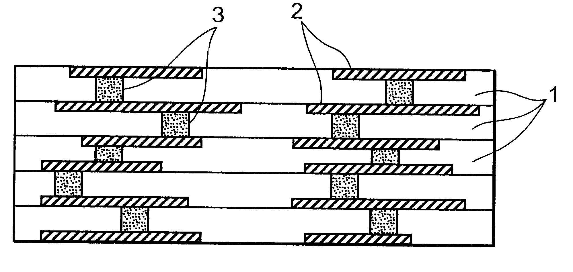
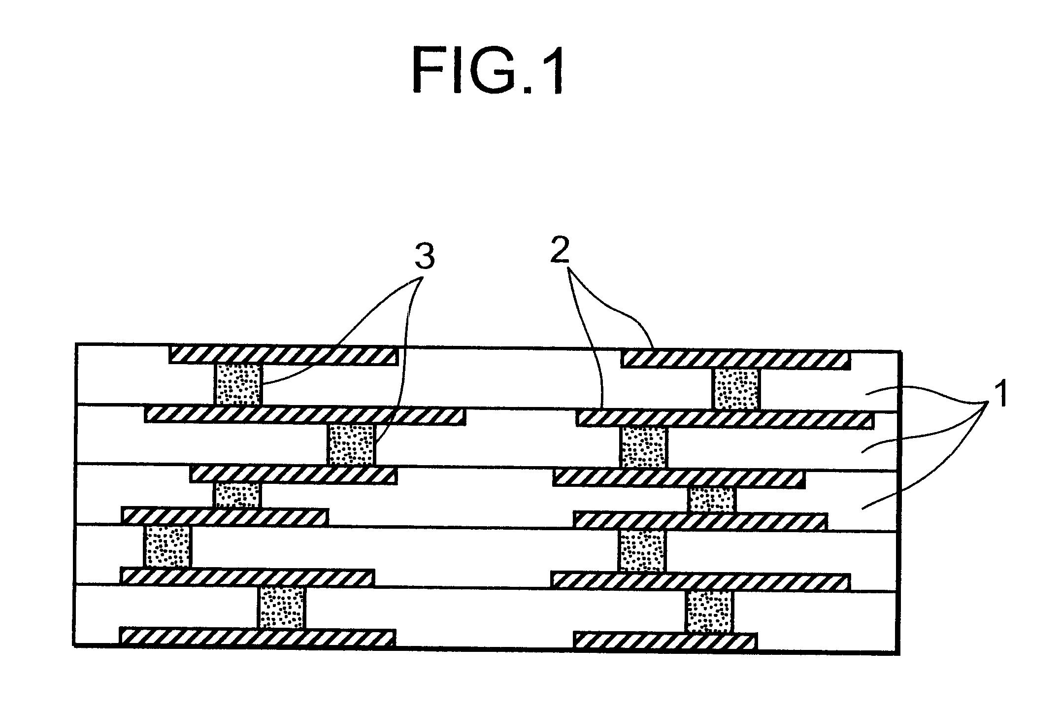
Multi-layer wiring board and method of producing the same
a wiring board and multi-layer technology, applied in the direction of insulating substrate metal adhesion improvement, printing element electric connection formation, transportation and packaging, etc., can solve the problem of low polarity of resin which absorbs water little, low polarity of resin, and poor wettability of metal surface of metal with high polarity, etc. problem, to achieve the effect of reducing the thickness reducing the resistance of the wire board, and improving the adhesion of the metal
- Summary
- Abstract
- Description
- Claims
- Application Information
AI Technical Summary
Benefits of technology
Problems solved by technology
Method used
Image

Examples
experiment 2
(Fabrication of the Multi-layer Wiring Board)
The following materials were used as insulating sheets for forming the insulating layers.
A prepreg comprising a glass fabric and an arylated polyphenylene ether resin (A-PPE resin);
A prepreg comprising a glass fabric and a BT resin;
A sheet in the B-stage having a thickness of 40 .mu.m prepared by using a resin composition containing the A-PPE resin and the spherical silica (inorganic filler) at a volume ratio of 50:50 relying upon the doctor blade method; and
A sheet in the B-stage having a thickness of 40 .mu.m prepared by using the BT resin and the spherical silica (inorganic filler) at a volume ratio of 50:50 relying upon the doctor blade method;
Via-conductors were formed in the above insulating sheets in the same manner as in Experiment 1.
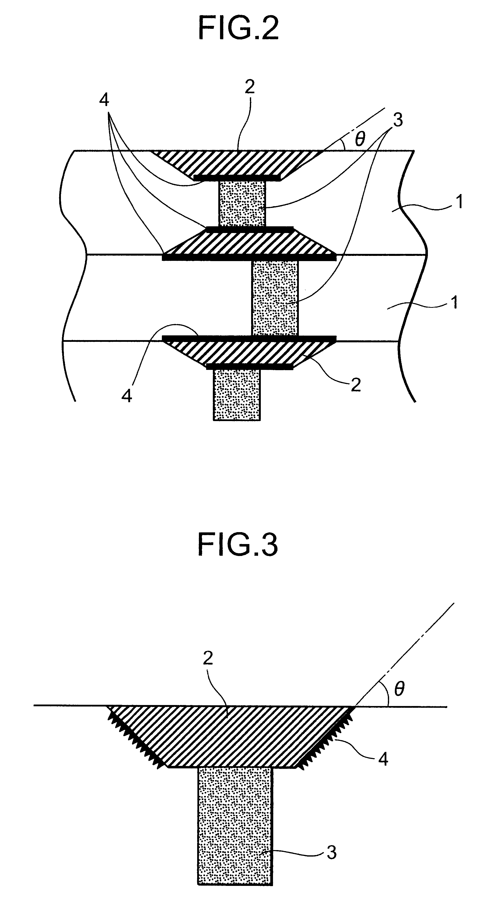
A conductor wiring layer of a trapezoidal shape with a side surface of an angle of inclination of 45.degree. to 80.degree. was formed on the PET film in the same manner as in Experiment 1 by using a f...
experiment 1
Like in Experiment 1, the thus obtained multi-layer wiring boards were measured concerning the water-absorbing factors of the thermosetting resins in the insulating sheets, and were evaluated for their electric conduction (proportion defective in the high-temperature standby testing and PCT testing). The results were shown in Table 3 together with the surface roughness (Ra) of the side surfaces of the conductor wiring layers and the angles of inclination of side surfaces of the conductor wiring layers. Surface roughness of the side surfaces of the conductor wiring layers were measured by using an atomic force microscope (AFM), and the angles of inclination of side surfaces of the conductor wiring layers were measured by observing the cross section of the conductor wiring layers by using the SEM.
As will be understood from the results of Table 3, by forming the coupling layers on the side surfaces of the conductor wiring layer, by setting the angle (.theta.) of inclination of the side...
PUM
| Property | Measurement | Unit |
|---|---|---|
| Ra | aaaaa | aaaaa |
| thickness | aaaaa | aaaaa |
| particle diameter | aaaaa | aaaaa |
Abstract
Description
Claims
Application Information