Multi-layer wiring board and method of producing the same

a wiring board and multi-layer technology, applied in the direction of insulating substrate metal adhesion improvement, printing element electric connection formation, transportation and packaging, etc., can solve the problem of low polarity of resin which absorbs water little, low polarity of resin, and poor wettability of metal surface of metal with high polarity, etc. problem, to achieve the effect of reducing the thickness reducing the resistance of the wire board, and improving the adhesion of the metal

Inactive Publication Date: 2002-11-07
KYOCERA CORP
View PDF0 Cites 45 Cited by
  • Summary
  • Abstract
  • Description
  • Claims
  • Application Information

AI Technical Summary

Problems solved by technology

According to the base+build-up method (1), however, the photosensitive epoxy resin used for forming the insulating layer has a low glass transition point and is sensitive to light involving such a defect that it absorbs water much.
That is, when left to stand under high-temperature and high-humidity conditions, the multi-layer wiring substrate obtained according to this method arouses a problem of decreased insulation.
However, the resin which absorbs water little has a low polarity and exhibits poor wettability to the surface of a metal which has a high polarity.
That is, with the multi-layer wiring board in which the insulating layer is formed of a resin that absorbs little water, the adhesion or intimate contact is not accomplished between the insulating layer and the conductor wiring layer, very easily permitting the passage of water that is a factor for deteriorating the characteristics of the wiring board.
When the diameter of the through-holes forming the via-conductors is decreased, further, a problem such as an increase in the resistance of the via-conductors appears conspicuously making it very difficult to fabricate a highly dense wiring board.
Such a multi-layer wiring board is not suited for the applications wh...

Method used


Image

  • Multi-layer wiring board and method of producing the same
  • Multi-layer wiring board and method of producing the same
  • Multi-layer wiring board and method of producing the same

Examples


experiment 1

[0086]

[0087] An arylated polyphenylene ether resin (A-PPE) or a BT resin was used as a thermosetting resin and a spherical silica was used as an inorganic filler.

[0088] A resin composition was prepared containing the above thermosetting resin and the inorganic filler at a volume ratio of 50:50, and from which an insulating sheet in the B-stage having a thickness of 40 .mu.m was prepared based on the doctor blade method.

[0089] By using a CO.sub.2 laser, through-holes having a diameter of 100 .mu.m or 50 .mu.m were formed in the insulating sheet. Then, the through-holes were filled with an electrically conducting paste obtained by mixing a copper powder of which the surfaces are coated with silver and a binder, thereby to prepare an insulating sheet B for forming an insulating layer.

[0090] On the other hand, a film with a copper foil for transfer was prepared by sticking an electrolytic copper foil of a thickness of 12 .mu.m to a PET film of a thickness of 38 .mu.m. A dry film resist ...

experiment 2

[0107]

[0108] (Fabrication of the Multi-layer Wiring Board)

[0109] The following materials were used as insulating sheets for forming the insulating layers.

[0110] A prepreg comprising a glass fabric and an arylated polyphenylene ether resin (A-PPE resin);

[0111] A prepreg comprising a glass fabric and a BT resin;

[0112] A sheet in the B-stage having a thickness of 40 .mu.m prepared by using a resin composition containing the A-PPE resin and the spherical silica (inorganic filler) at a volume ratio of 50:50 relying upon the doctor blade method; and

[0113] A sheet in the B-stage having a thickness of 40 .mu.m prepared by using the BT resin and the spherical silica (inorganic filler) at a volume ratio of 50:50 relying upon the doctor blade method;

[0114] Via-conductors were formed in the above insulating sheets in the same manner as in Experiment 1.

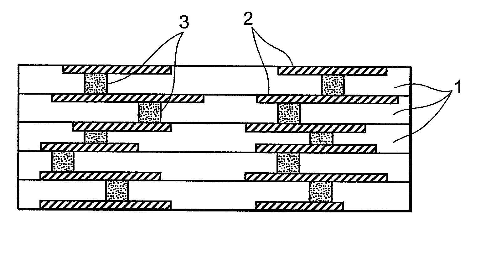
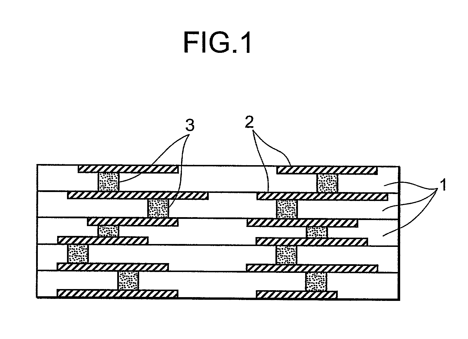
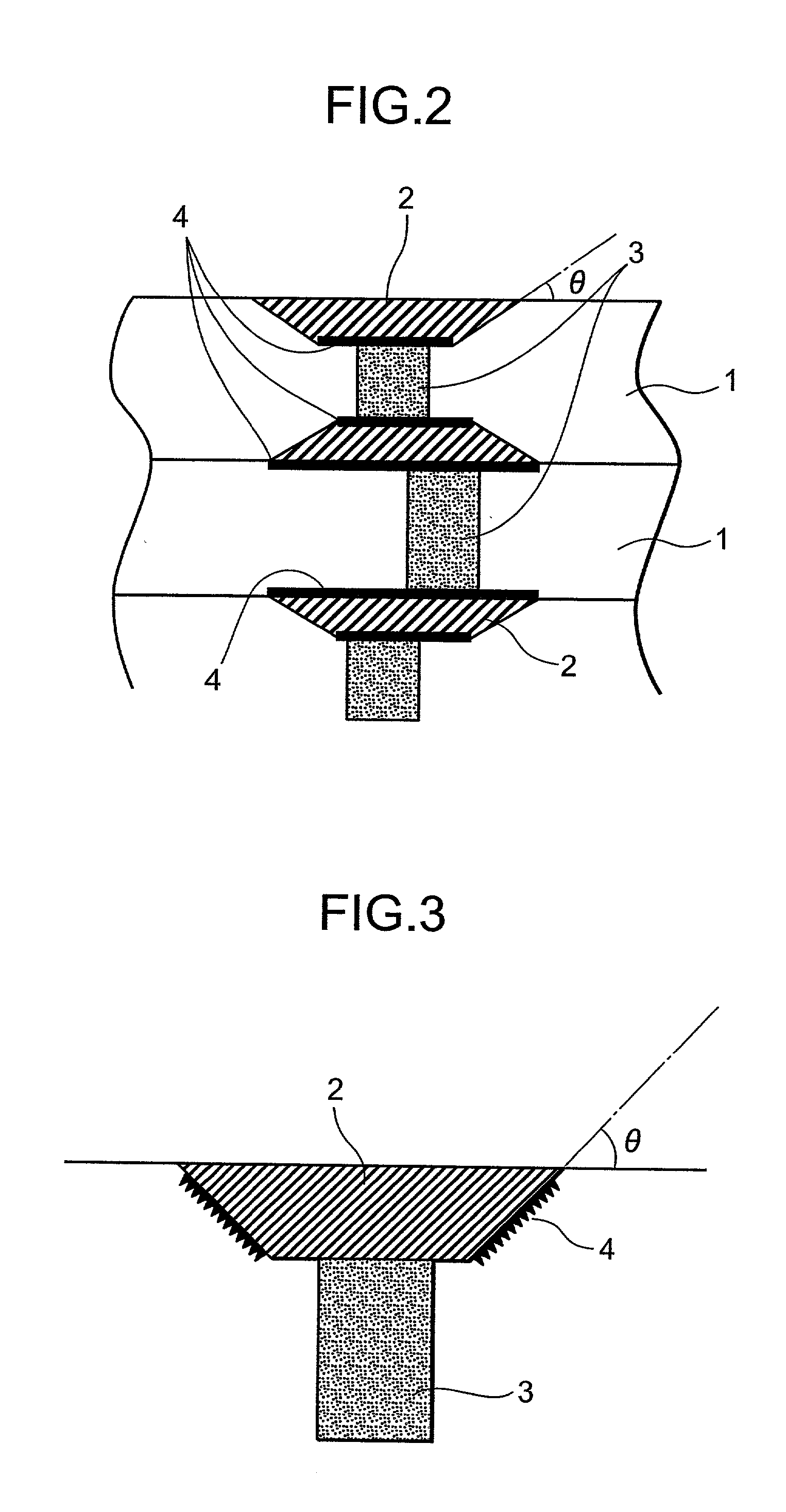
[0115] A conductor wiring layer of a trapezoidal shape with a side surface of an angle of inclination of 45.degree. to 80.degree. was formed on t...


PUM

PropertyMeasurementUnit
Fractionaaaaaaaaaa
Thicknessaaaaaaaaaa
Angleaaaaaaaaaa

Abstract

Disclosed is a multi-layer wiring board comprising insulating layers of a thermosetting resin having through-holes formed therein, conductor wiring layers buried in the surfaces of said insulating layers, and via-conductors formed by filling said through-holes with an electrically conducting paste, the via-conductors being electrically connected to said conductor wiring layers, wherein coupling layers comprising a silane coupling agent are formed in the interfaces between said conductor wiring layers and said via-conductors or said insulating layers. The multi-layer wiring board features an increased chemical affinity between the conductor wiring layer and the insulating layer, effectively suppressing the infiltration of water through the interface between the conductor wiring layer and the insulating layer or through the insulating resin, and effectively preventing deterioration in the properties under a high-temperature and high-humidity environment of an extended period of time.

Description

BACKGROUNG OF THE INVENTION[0001] 1. Field of the Invention[0002] The present invention relates to a multi-layer wiring board suited for a package for holding a semiconductor device and to a method of producing the same.[0003] 2. Description of the Related Art[0004] In recent years, electronic equipment have been produced in ever small sizes. Recent development of portable data terminals and widespread use of a so-called mobile computing operated while carrying a computer with the user, are further demanding a multi-layer wiring board fabricated in a further decreased size, in a more reduced thickness and having more highly dense wiring layers.[0005] There have further been widely used electronic equipment that must operate at high speeds as represented by communication equipment. The demand for a high-speed operation includes a variety of requests such as precise switching for the signals of high frequencies. To cope with such electronic equipment, it has been urged to provide a mu...

Claims


Application Information

Patent Timeline
IPC IPC(8): H05K3/20H05K3/38H05K3/40H05K3/46
CPCH05K3/20H05K3/389H05K3/4069H05K3/4617H05K2201/0239Y10T428/24917Y10T428/24942Y10T428/24967Y10T29/49126Y10T29/49128Y10T29/49165H05K2203/1461Y10T428/31663Y10T428/31692
Inventor AKIHIKO, NISHIMOTO
Owner KYOCERA CORP
Why Eureka
Try Eureka