Transfer film and process for producing organic electroluminescent device using the same

a technology of transfer film and electroluminescent device, which is applied in the manufacture of electromechanical devices, photographic processes, electric lighting sources, etc., can solve the problems of difficult pattern formation, easy damage to organic materials composing organic electromechanical devices, corrosion or degradation

Inactive Publication Date: 2004-10-19
SHARP KK
View PDF16 Cites 224 Cited by
  • Summary
  • Abstract
  • Description
  • Claims
  • Application Information

AI Technical Summary

Problems solved by technology

However, an organic material composing the organic EL device is susceptible to damages such as a corrosion or degradation in characteristic due to organic solvent, water, oxygen or the like.
Therefore, it is generally difficult to form a pattern by a general photolithography method once a layer containing an organic material is formed.
However, the method for forming a pattern formation by the vapor-deposition is not considered to be satisfactory from the viewpoint of production because of the following reasons such that it is difficult to achieve a high precision of the pattern, it is difficult to perform an alignment of a mask with a throwing power considered or the process becomes complicated.
Further, the mask vapor-deposition method has a problem that it is difficult to vapor-deposit onto a large-sized substrate, while the ink jet method has a problem of declining productivity since it takes much time to perform the pattern formation by using a large-sized substrate.
However, the aforesaid conventional technique has following problems.
In the case of transferring the multi-layer in the conventional pattern formation method using the transfer method, a satisfactory transfer cannot sometimes be executed due to a difference in melting point of each layer or a laminating order.
Further, even when the satisfactory transfer can be obtained, the transfer layer suffers damages from heat if the temperature greatly rises upon transferring, thereby entailing a problem of deteriorating the transfer layer.

Method used


Image

  • Transfer film and process for producing organic electroluminescent device using the same
  • Transfer film and process for producing organic electroluminescent device using the same
  • Transfer film and process for producing organic electroluminescent device using the same

Examples


example 1

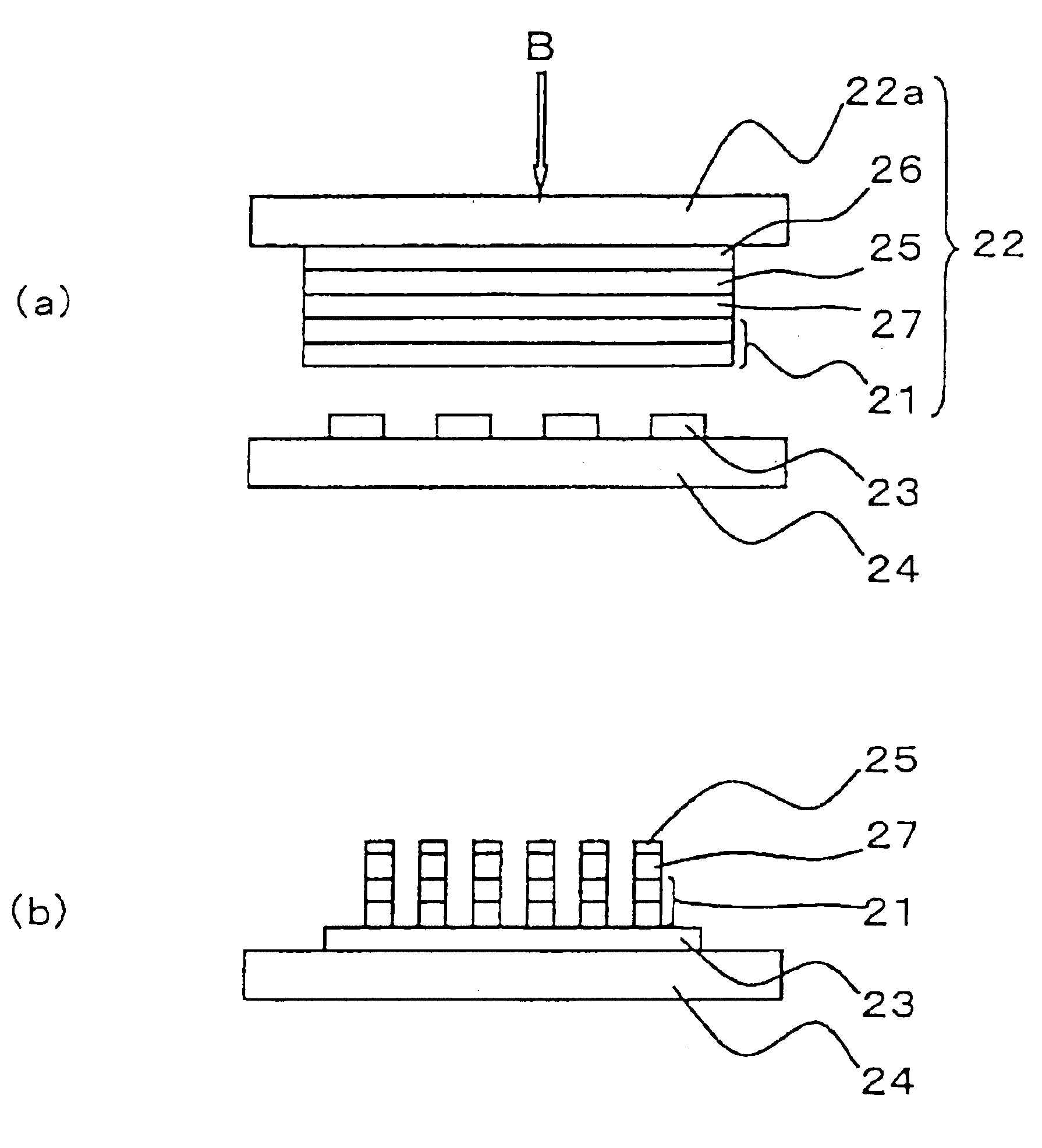
Polyethylene terephthalate with a thickness of 150 .mu.m was used as a base film. Formed thereon was a layer of stearic acid with a thickness of 100 nm by a vapor-deposition method as a transfer auxiliary layer. The melting point of stearic acid was 68.degree. C. Further, (8-hydroxyquinolinato) aluminum complex (Alq.sub.3) (melting point: 413.degree. C., glass transition temperature: 175.degree. C.) serving as the organic light-emitting layer and N,N'-di(naphthalene-1-yl)-N,N'-diphenyl-bendizine (NPD) (melting point: 275.degree. C., glass transition temperature: 95.degree. C.) serving as the hole transporting material were formed by the vapor-deposition method, each having a thickness of 50 nm. The transfer film thus manufactured was attached to a glass substrate that was patterned in advance to have a transparent electrode formed thereon. A linear heat source (e.g., nichrome line through which electric current flows) was pushed to the resultant from the base film side for fusing th...

example 2

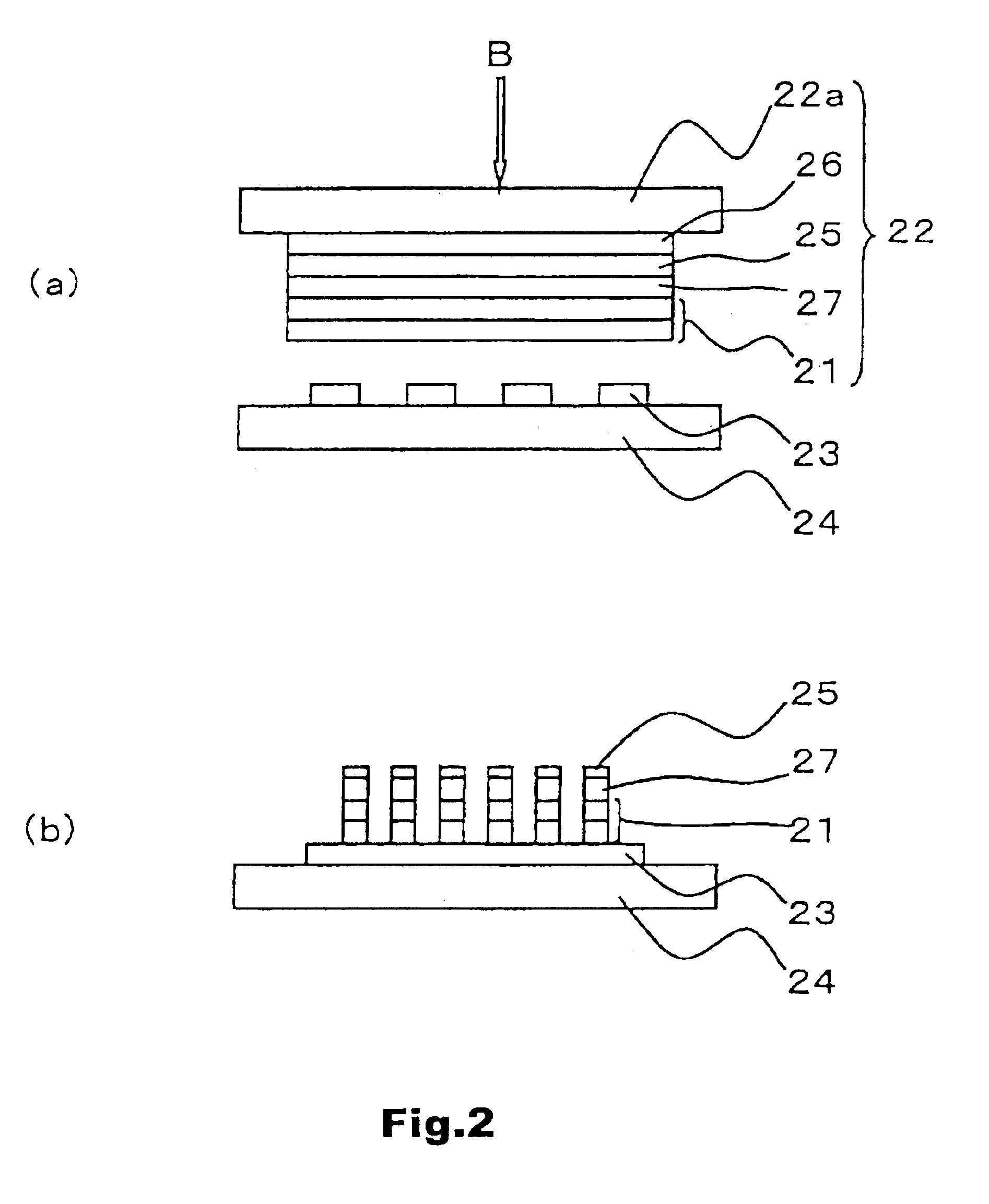
A transfer was performed by the same manner as in the Example 1 except that any one of a multi-layer film of Al layer / Alq.sub.3 layer / NPD layer, a multi-layer film of light transmitting metal thin-film Al layer / Alq.sub.3 layer / NPD layer and a multi-layer film of transparent conductive layer / NPD layer / Alq.sub.3 layer was used for the transfer layer. A satisfactory transfer could also be obtained. Transferring simultaneously an electrode layer enabled reduction in the number of process.

Generally, materials used for the electrode layer are inorganic and have a greater hardness than organic materials. Therefore, their thickness is preferably thin in order to perform a satisfactory transfer. Moreover, the structure of the multi-layer film of metal thin-film Al layer / Alq.sub.3 layer / NPD layer or the multi-layer film of transparent conductive film layer / NPD layer / Alq.sub.3 layer enables to take the emission from the side opposite to the substrate, whereby the decrease of aperture ratio can...

example 3

Polyethylene terephthalate with a thickness of 150 .mu.m was used as a base film. Formed thereon as a light-to-heat conversion layer was a layer in which carbon black was dispersed in a polymer material. The transfer auxiliary layer, hole transporting layer and light-emitting layer were formed by the same manner as in Example 1. The transfer film thus manufactured was attached to a glass substrate that was patterned in advance to have a transparent electrode formed thereon. Laser light was irradiated to the resultant from the base film side for fusing the transfer auxiliary layer by utilizing the heat at the light-to-heat conversion layer, whereby the transfer layer was pattern-transferred onto the glass substrate having the transparent electrode formed thereon. Power of the laser light was optionally selected to thereby obtain a satisfactory transfer layer. A cathode was formed after the transfer on the transfer layer, with the result that a green light emission from Alq.sub.3 was ...


PUM

PropertyMeasurementUnit
thicknessaaaaaaaaaa
thicknessaaaaaaaaaa
thicknessaaaaaaaaaa

Abstract

A transfer film comprising a base film, a transfer layer, and a transfer auxiliary layer formed between the base film and the transfer layer so as to be in contact with at least the transfer layer, this transfer auxiliary layer having a melting point or a glass transition temperature lower than that of the transfer layer, wherein at least a portion of the transfer layer can be thermally transferred onto a substrate.

Description

This application is related to Japanese Patent Application No. 2001-148587 filed on May 18, 2001 whose priority is claimed under 35 USC .sctn. 119, the disclosure of which is incorporated by reference in its entirety.1. Field of the InventionThe present invention relates to a transfer film and a process for producing an organic electroluminescent device using the same.2. Description of the Prior ArtsRecently, there is more need for a flat panel display as a thin and light-weight display device with reduced power consumption, compared to a cathode-ray tube (CRT).Known as the flat panel display device are a non-luminous liquid crystal display (LCD), a self-luminous plasma display panel (PDP), an electroluminescent (EL; referred to as EL hereafter) display or the like.Among these displays, the EL display is classified into two types, i.e., an inorganic EL display and an organic EL display, from the viewpoint of a difference in its luminous mechanism and component materials. Particularl...

Claims


Application Information

Patent Timeline
Patent Type & Authority Patents(United States)
IPC IPC(8): H01L27/32H01L27/28H01L51/40H01L51/05H01L51/30H01L51/00B44C1/17H01L51/50H05B33/10H05B33/28
CPCH01L51/0013H01L27/32H01L27/3244H01L51/0004Y10T428/24942H01L51/0059H01L51/0081Y10S428/917H10K71/13H10K71/18H10K59/12H10K85/631H10K85/324H10K59/00
Inventor OGURA, TAKASHIYAMANA, SHINJIAKAI, TOMONORI
Owner SHARP KK
Why Eureka
Try Eureka