Electrically conductive organic compound and electronic device

a technology of organic compound and electric conductive, which is applied in the direction of conductive materials, solid-state devices, non-conductive materials with dispersed conductive materials, etc., can solve the problems of limited application of such a technology to a small percentage, not yet spread widely, and further lowering mobility

Inactive Publication Date: 2005-08-30
FUJITSU LTD
View PDF10 Cites 61 Cited by
  • Summary
  • Abstract
  • Description
  • Claims
  • Application Information

AI Technical Summary

Benefits of technology

[0017]As will be explained in detail hereinafter, the present invention introduces a π conjugated system skeletal structure into a main chain of molecules of an electrically conductive organic compound as a starting compound, and at the same time introduces a molecule having refractive index anisotropy (in other words, orientation property and liquid crystal property) contributing to molecular orientation and σ conjugated type electrical conductivity as the side chain of the molecules. Accordingly, the present invention can simultaneously improve orientation of the π conjugated type main chain and conductivity of the side chain, and can also improve field effect mobility. In addition, whenever necessary, a substitution group such an alkyl group can be introduced into the molecules, too, so as to improve solubility in a solvent within the range where the effect of the invention is not impeded. When excellent solubility in the solvent can be secured by the introduction of the substitution group, an electronic device having desired performance can be produced by an easy process, that forms a thin film from a solution, such as the casting method and the printing method, without deteriorating high field-effect mobility.
is not impeded. When excellent solubility in the solvent can be secured by the introduction of the substitution group, an electronic device having desired performance can be produced by an easy process, that forms a thin film from a solution, such as the casting method and the printing method, without deteriorating high field-effect mobility.

Problems solved by technology

In existing electronic circuits mainly using polycrystalline silicon (poly-Si) and amorphous silicon (a-Si), however, large-scale processes such as those including application of high-temperature and high-vacuum processes are necessary, and therefore, the application of such a technology is limited to only a small percentage in the production of portable devices and has not yet spread widely, in view of insufficient heat resistance of the plastic substrate used and the production cost.
Further, generally, when the film is formed from the solution, the field effect mobility is further lowered in the order of 1 to 2 figures or location of number because of difficulties in molecular orientation control.
In other words, the greatest problem for practical utilization of the organic semiconductors is how to accomplish high field effect mobility through a simple fabrication process.
However, orientation restrictive force by the orientation film is weak in the organic semiconductor molecule not having crystallinity, and sufficient molecular orientation is not accomplished.

Method used


Image

  • Electrically conductive organic compound and electronic device
  • Electrically conductive organic compound and electronic device
  • Electrically conductive organic compound and electronic device

Examples


application examples

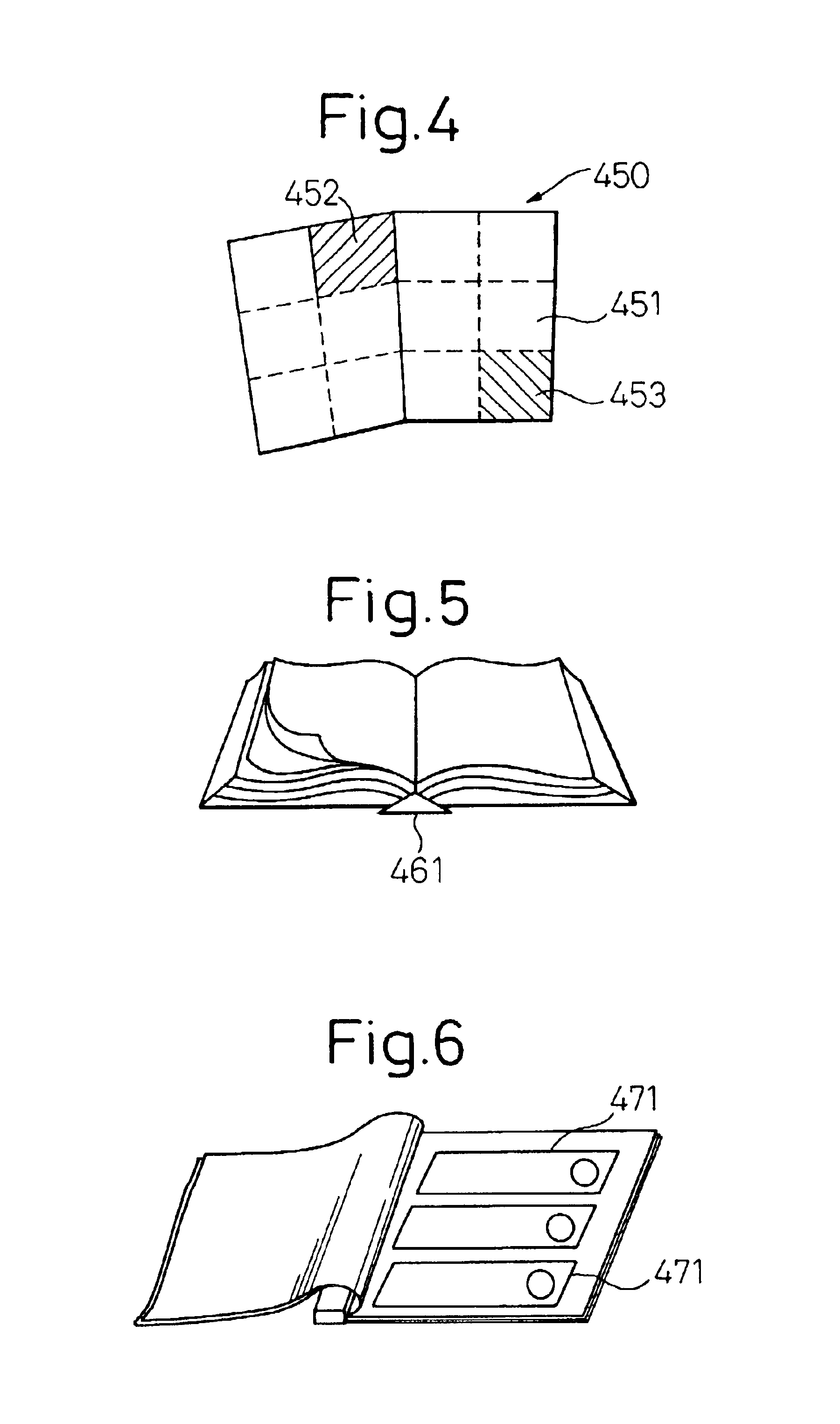
[0143]FIG. 6 shows an outline of the device. The electronic catalog has input means such as a touch key or an electronic pen, and displays merchandise information 471. Necessary fields are in advance registered for the merchandise information, and are automatically updated upon receipt of an update report by communication. The screen can be switched to display of the merchandise list to the detailed information. When only the switch is operated on the basis of the individual information that is default-inputted by the communication function, order can be placed and electronic settlement is made from the registered bank account. Retrieval and display of various merchandises other than those of the registered fields can be made, and order form them can also be placed.

[0144](2) Display board (electronic bulletin) system that can be put on the wall and can be removed therefrom, and automatically receives and updates the local information:

Form Example:

[0145]From A4 to A3 size (foldable t...

example of form

[0239]at least A4 size.

Example of Functions:

[0240]transmission / reception, data memory, screen switching, enlargement / reduction, input, retrieval, video input, etc.

Examples of Constituent Elements:

[0241]display portion, driving circuit, power source, communication (transmission / reception) circuit, control circuit, memory, input means, video input means, etc.

application example

[0242]FIG. 17 shows an example of the display device for the global education system. Here, the global education system includes an electronic blackboard 581 similar to the display device of the electronic conference system (7) and a display device 582 similar to the electronic text (19). This system can transmit, display and record the content a teacher puts on the electronic blackboard 581 while keeping linkage with schools in the world. The system can also assist individual teaching between the teacher and the student. An audio input / output function and a video input function may be added to this system.

[0243]Next, a structural example of the sheet-like display device according to the invention that uses the electrically conductive resin layer as a common electrode positioned on the display surface side will be explained with reference to FIG. 18.

[0244]As shown in FIG. 18, the sheet-like display device 700 comprises discrete electrodes 702 formed on a substrate 701, microcapsules...


PUM

PropertyMeasurementUnit
conductivityaaaaaaaaaa
condensation timeaaaaaaaaaa
thicknessaaaaaaaaaa

Abstract

In an electrically conductive organic compound, a side chain portion simultaneously exhibiting refractive index anisotropy and σ conjugated system electrical conductivity is bonded to a main chain portion exhibiting π conjugated system electrical conductivity. The electrically conductive organic compound is used in the production of a constituent element for electronic devices.

Description

CROSS-REFERENCE TO RELATED APPLICATIONS[0001]This application is based upon and claims a priority of Japanese Patent Application No. 2001-317096, filed Oct. 15, 2001, the contents being incorporated herein by reference.BACKGROUND OF THE INVENTION[0002]1. Field of the Invention[0003]The present invention relates to an electrically conductive organic compound. More particularly, the present invention relates to an organic semiconductor that can be used for the production of electronic devices such as transistors and, specifically to an organic semiconductor that can be applied to flexible electronic devices such as electronic paper. The present invention also relates to an electronic device using such an organic semiconductor.[0004]2. Description of Related Art[0005]Performance of liquid crystal displays and organic EL displays has been drastically improved in recent years in the field of electronic displays, and a remarkable progress has been made in high precision and large scale di...

Claims


Application Information

Patent Timeline
Patent Type & Authority Patents(United States)
IPC IPC(8): C08G61/12C08G61/00H01B1/12H01L51/05H01L51/30H01L51/50C08G77/60H01L29/786
CPCC08G61/126H01B1/127H01L51/0036H01L51/0094H01L51/0545H10K85/113H10K85/40H10K10/466C08G61/12
Inventor YOSHIDA, HIROAKI
Owner FUJITSU LTD
Why Eureka
Try Eureka