Semiconductor integrated circuit device

a technology of integrated circuits and semiconductors, applied in semiconductor devices, digital storage, instruments, etc., can solve the problems of data disappearance danger, inability to enhance the write margin, etc., and achieve the effect of enhancing the write margin to memory cells

Active Publication Date: 2006-09-26
RENESAS ELECTRONICS CORP
View PDF3 Cites 95 Cited by
  • Summary
  • Abstract
  • Description
  • Claims
  • Application Information

AI Technical Summary

Benefits of technology

[0009]Provided with the above construction, the invention achieves enhancing the write margin to the memory cells corresponding to the selected complimentary bit lines, and it also achieves securing the SNM to the non-selected memory cells connected to the non-selected complimentary bit lines.

Problems solved by technology

The technique of the Patent Document 1 involves lowering the internal supply voltage supplied to the memory cells of which the word lines selected by the row decoder are activated, which are not selected by the column decoder, and it also involves the danger of disappearing data because of the influences of noises in the read-out state of the lowered SNM.
However, to generate such a lower limit voltage, the technique needs to provide an intermediate supply voltage generator inside the memory.
This provision of the intermediate supply voltage generator increases the current consumption of the memory circuit, and the lower limit voltage restrains the lowering of the SNM, thus leading to incapability of enhancing the write margin.

Method used


Image

  • Semiconductor integrated circuit device
  • Semiconductor integrated circuit device
  • Semiconductor integrated circuit device

Examples


Embodiment Construction

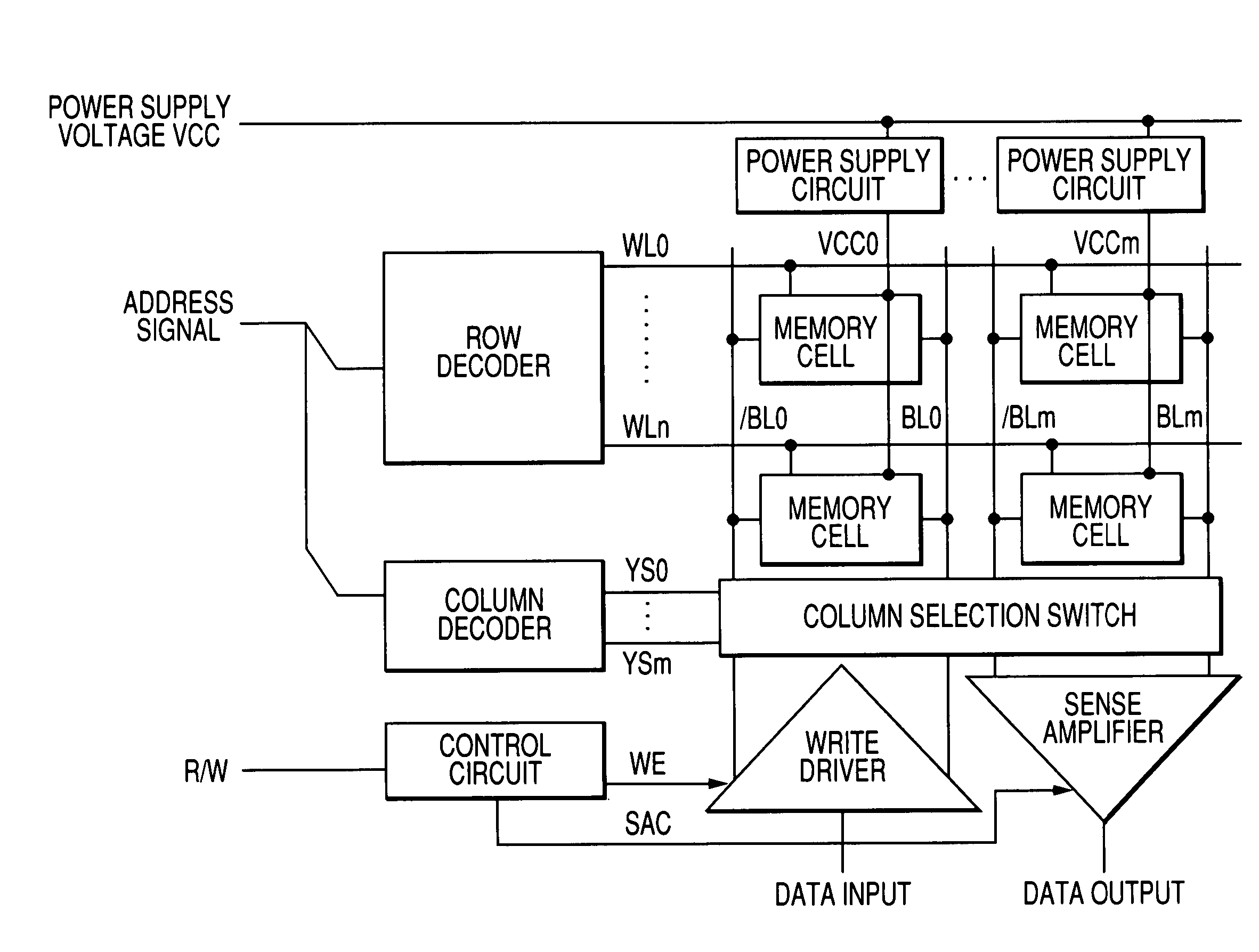
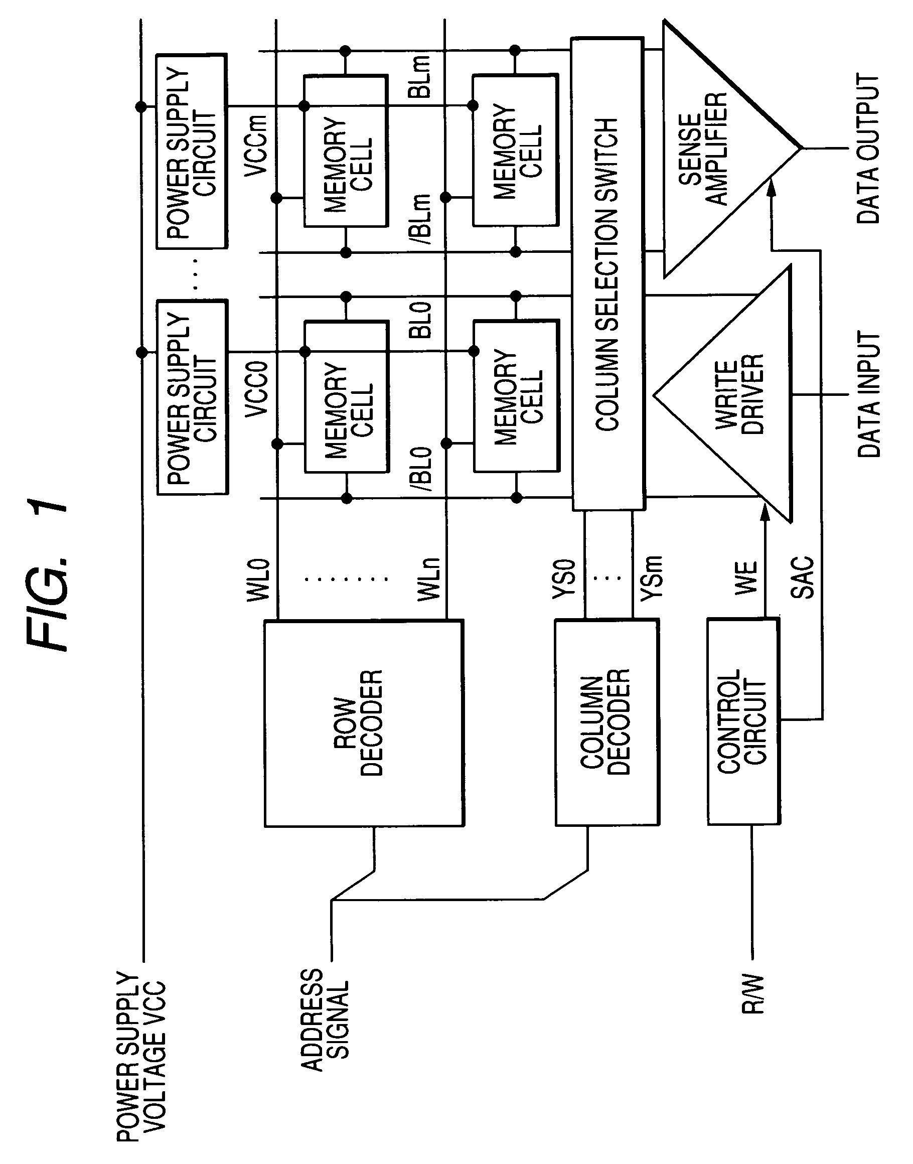
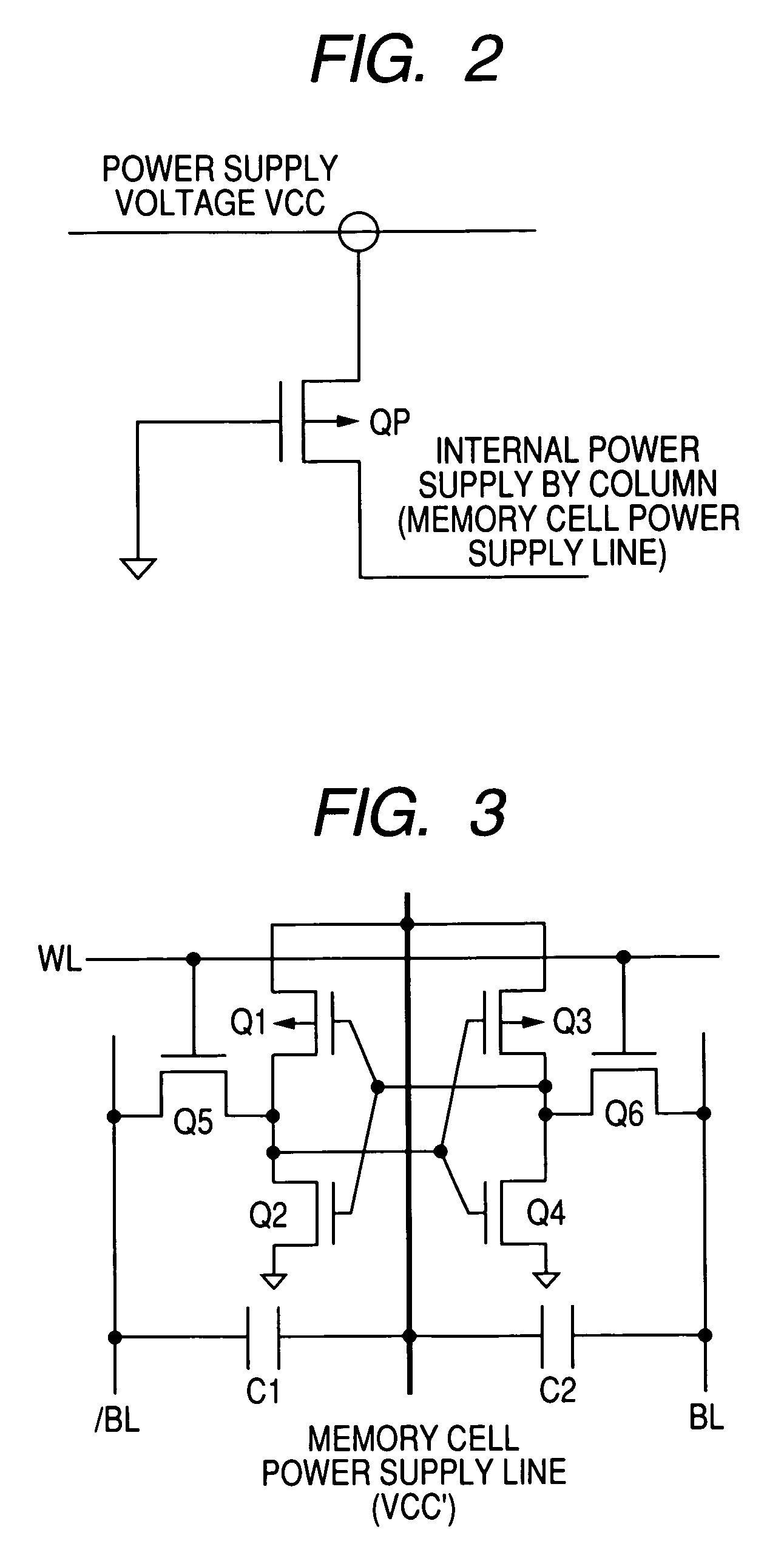
[0029]FIG. 1 illustrates a circuit configuration of the SRAM as one embodiment relating to this invention. The drawing typically illustrates four memory cells, and two word lines WL0 and WLn and complimentary bit lines / BL0, BL0 and / BLm, BLm, which corresponds to the four memory cells. The memory cell, which is not illustrated here, includes two CMOS inverters composed of P-channel MOSFETs and N-channel MOSFETs, of which inputs and outputs are cross-connected to form a latch circuit as a memory unit and mutually connected input / output points are used as the memory nodes, and N-channel MOSFETs for address selection, which are provided between the corresponding bit lines / BL and BL. The gates of the MOSFETs for address selection are connected to the corresponding word lines.

[0030]One of the word lines WL0 through WLn is selected by a row decoder. The row decoder includes a word driver, which will be described later. The row decoder is supplied with the row-system address signals of t...


PUM


Abstract

The invention provides a semiconductor integrated circuit device provided with an SRAM that satisfies the requirements for both the SNM and the write margin with a low supply voltage. The semiconductor integrated circuit device include: multiple static memory cells provided in correspondence with multiple word lines and multiple complimentary bit lines; multiple memory cell power supply lines that each supply an operational voltage to each of the multiple memory cells connected to the multiple complimentary bit lines each; multiple power supply circuits comprised of resistive units that each supply a power supply voltage to the memory cell power supply lines each; and a pre-charge circuit that supplies a pre-charge voltage corresponding to the power supply voltage to the complimentary bit lines, wherein the memory cell power supply lines are made to have coupling capacitances to thereby transmit a write signal on corresponding complimentary bit lines.

Description

CROSS-CONFERENCE TO RELATED APPLICATION[0001]The present application claims priority from Japanese patent application No. 2004-267645 filed on Sep. 15, 2004, the content of which is hereby incorporated by reference into this application.BACKGROUND OF THE INVENTION[0002]The present invention relates to a semiconductor integrated circuit device, specifically to a technique effective in use for a semiconductor integrated circuit device provided with a static random access memory.[0003]As one of the parameters for evaluating the memory cells of a static random access memory (hereunder, simply referred to as SRAM), the static noise margin (hereunder, simply referred to as SNM) is generally used. The SNM indicates the stability of data stored in the memory cells. As the value of the SNM becomes increased, the data retaining operation of the memory cells becomes more stabilized; on the contrary however, the writing of inverse data to the retained data stored in the memory cells becomes dif...

Claims


Application Information

Patent Timeline
Patent Type & Authority Patents(United States)
IPC IPC(8): G11C11/00
CPCG11C5/063G11C5/14H01L27/1104G11C11/419H01L27/11G11C11/412H10B10/00H10B10/12H10B99/00
Inventor MAEDA, NORIAKISHINOZAKI, YOSHIHIROYAMAOKA, MASANAOSHIMAZAKI, YASUHISAISODA, MASANORINII, KOJI
Owner RENESAS ELECTRONICS CORP
Why Eureka
Try Eureka