Semiconductor memory device

a technology of semiconductor memory and design technique, which is applied in the direction of information storage, static storage, digital storage, etc., can solve the problems of increasing the probability of occurrence of the requirements of the layout area, so as to prevent a timing mismatch in data input, reduce the total number of multiplexers, and simplify input to the multiplexers

Inactive Publication Date: 2006-12-19
SK HYNIX INC
View PDF4 Cites 1 Cited by
  • Summary
  • Abstract
  • Description
  • Claims
  • Application Information

AI Technical Summary

Benefits of technology

[0013]It is, therefore, a primary object of the present invention to provide a semiconductor memory device, which is capable of further simplifying the data multiplexing structure on a data write path, thereby preventing a timing mismatch in data input from being occurred.
[0015]In the present invention, a scheme is employed, which disposes a data multiplexing structure for the data width option at the side of a main write driver. Specifically, the scheme is not multiplexing data applied to the data input / output pins (DQ) but multiplexing data carried on the global I / O buses (GIO). In this case, the total number of the multiplexers is decreased, and input to the multiplexers is simplified, thereby resulting in a dramatically reduced layout area and preventing a timing mismatch in data input from being occurred.

Problems solved by technology

As can be seen from FIG. 1, the prior art suffers from the disadvantage that the data multiplexers MUX ×4 and MUX ×8 are intricately connected with the data input / output pins DQ0 to DQ15, resulting in greater layout area requirements.
Meanwhile, since several addresses should be inputted to control the data multiplexers MUX X4 and MUX X8 in synchronism with a data input timing, the prior art suffers from the disadvantage that the probability of occurrence of a timing mismatch in data input increases.

Method used


Image

  • Semiconductor memory device
  • Semiconductor memory device
  • Semiconductor memory device

Examples


Embodiment Construction

[0021]Hereinafter, a semiconductor memory device according to the present invention will be described in detail referring to the accompanying drawings

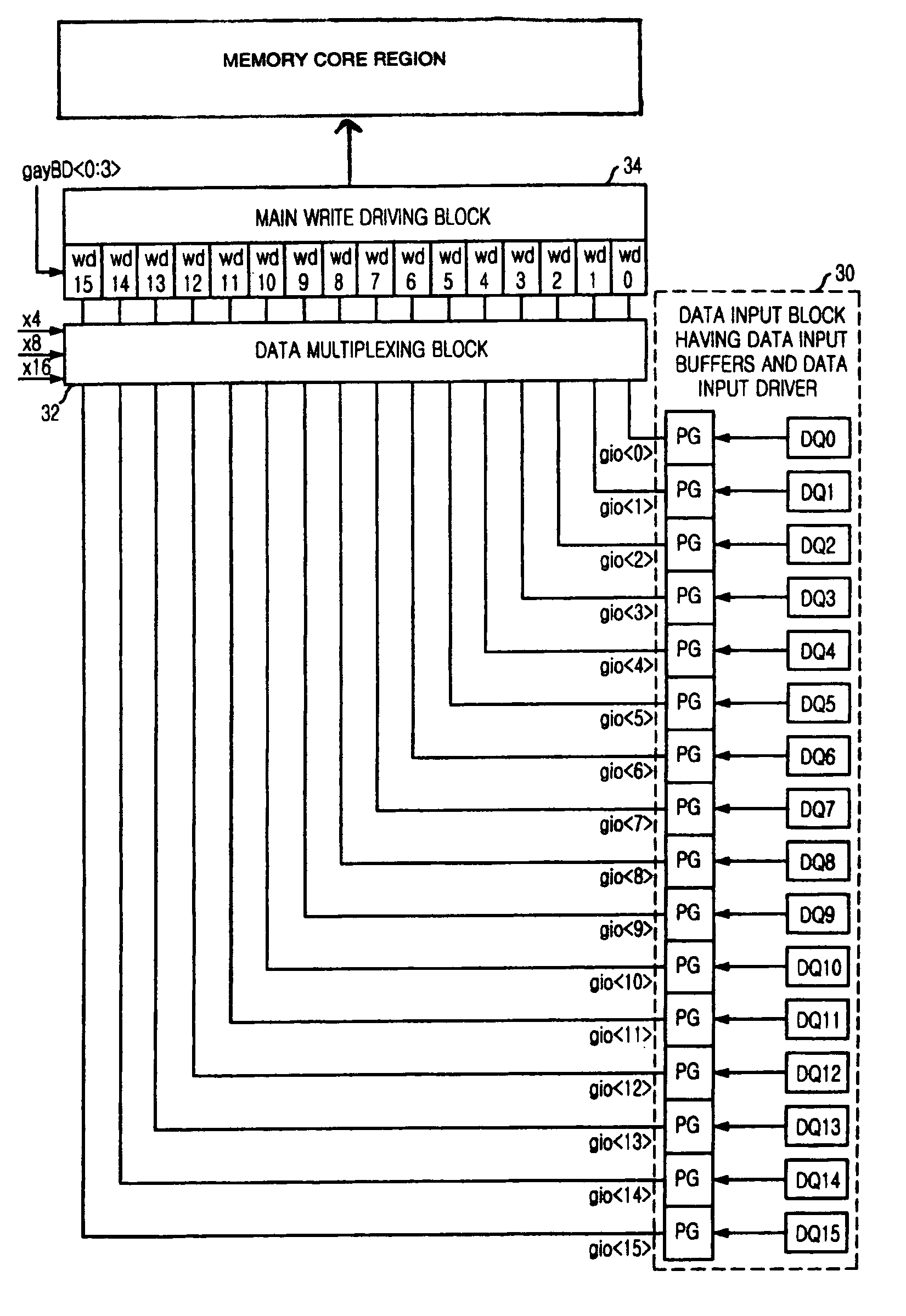
[0022]FIG. 3 is a block diagram of a data write path in accordance with a preferred embodiment of the present invention.

[0023]Referring to FIG. 3, the data write path in accordance with a preferred embodiment of the present invention comprises: a data input block 30 for transferring data applied to data input / output pins DQ0 to DQ15 to global I / O buses gio0:15>; a data multiplexing block 32 for multiplexing data carried on the global I / O buses gio0:15> according to data width options ×4, ×8 and ×16; and a main write driving block 34 for driving data outputted from the data multiplexing block 32 to a memory cell array (memory core region) in response to a control signal gayBD0:3>.

[0024]Herein, the data input block 30 includes the plurality of data input / output pins DQ0 to DQ15, a plurality of data input buffers (not shown) for buffering...


PUM


Abstract

Provided is a semiconductor memory device, which is capable of further simplifying the data multiplexing structure on a data write path, thereby preventing a timing mismatch in data input from being occurred. The semiconductor memory device, which comprises a data inputting block 30 for transferring data applied to a plurality of data input / output pins DQ0 to DQ15 to a plurality of global I / O buses gio<0:15>, a data multiplexing block 32 for multiplexing the data carried on the plurality of global I / O buses gio<0:15> according to a data width option, and a main write driver 34, in response to a control signal, for driving the data outputted from the multiplexing means to a memory core region.

Description

FIELD OF INVENTION[0001]The present invention relates to a design technique for a semiconductor memory device; and, more particularly, to a data write path of the semiconductor memory device.DESCRIPTION OF PRIOR ART[0002]Typically, a data bus, which transfers data inputted thereto via data input / output pins (DQ) to a memory cell array, is referred to as a global I / O bus (GIO). Included within the memory cell array is a hierarchical I / O bus structure for transferring data between each bit line and the global I / O bus.[0003]Meanwhile, a write driver is used to drive data carried on the global I / O bus to the I / O bus within the memory cell array, and an I / O sense amplifier (IOSA) is used to transfer the data carried on the I / O bus within the memory cell array to the global I / O bus.[0004]In addition, a data input buffer, a data multiplexer, a data input driver and the like are disposed at a region of peripheral circuitry to constitute a data write path of the semiconductor memory device. ...

Claims


Application Information

Patent Timeline
Patent Type & Authority Patents(United States)
IPC IPC(8): G11C7/10G11C8/00G11C11/40
CPCG11C7/1006G11C7/1048G11C7/1078G11C7/1096G11C11/40
Inventor SONG, SEONG-HWI
Owner SK HYNIX INC
Why Eureka
Try Eureka