Storage elements using nanotube switching elements

a switching element and nanotube technology, applied in digital storage, pulse technique, instruments, etc., can solve the problems of high power consumption, density and operation speed of mos digital circuits, and limited density of bipolar digital integrated circuits

Inactive Publication Date: 2007-01-09
NANTERO
View PDF40 Cites 165 Cited by
  • Summary
  • Abstract
  • Description
  • Claims
  • Application Information

AI Technical Summary

Problems solved by technology

However, the density of bipolar digital integrated circuits is limited by their high power consumption and the ability of packaging technology to dissipate the heat produced while the circuits are operating.
The density and operating speed of MOS digital circuits are still limited by the need to dissipate the heat produced when the device is operating.
Digital logic integrated circuits constructed from bipolar or MOS devices do not function correctly under conditions of high heat or extreme environments.
As leakage current increases, the operating temperature of the device rises, the power consumed by the circuit increases, and the difficulty of discriminating the off state from the on state reduces circuit reliability.
Conventional digital logic circuits also short internally when subjected to certain extreme environments because electrical currents are generated inside the semiconductor material.
It is possible to manufacture integrated circuits with special devices and isolation techniques so that they remain operational when exposed to such environments, but the high cost of these devices limits their availability and practicality.
In addition, such digital circuits exhibit timing differences from their normal counterparts, requiring additional design verification to add protection to an existing design.
Integrated circuits constructed from either bipolar or FET switching elements are volatile.
Alternative solutions to avoid losing information in volatile digital circuits, such as battery backup, also add cost and complexity to digital designs.

Method used


Image

  • Storage elements using nanotube switching elements
  • Storage elements using nanotube switching elements
  • Storage elements using nanotube switching elements

Examples


embodiment 600

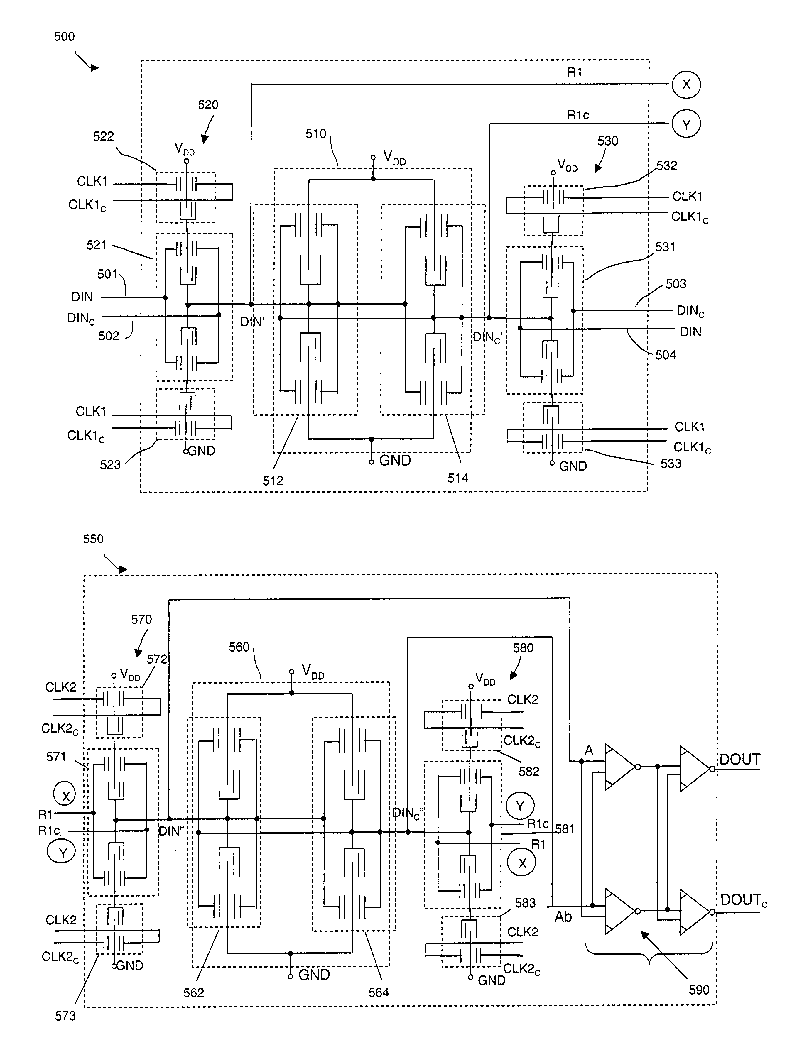
[0098]FIG. 6 is a schematic representation of a gated latch 600 that provides an alternate embodiment for master latch 500. In gated latch 600, a volatile three-terminal single-rail input nanotube-based transfer device 620, 630 is used in place of each tri-state inverter 520, 530 in master latch 500. In the illustrated embodiment, each volatile three-terminal single-rail input device 620 and 630 is constructed from a four-terminal nanotube switching element wherein the release electrode is connected to the signal electrode. Each volatile three-terminal single-rail input nanotube-based transfer device 620 and 630 has an input, Din and DinC, respectively, and an output to storage element 510. The transfer of the input from the signal electrode of each transfer device to the output electrode is controlled by CLK1. When CLK1 is high, transfer device 620 transfers the signal Din. The conductive channel is created by the deflection of the nanotube channel element when there is a sufficien...

embodiment 800

[0100]FIG. 8 is a schematic representation of a volatile single-rail tristate inverter 800 that can be used to replace each of non-volatile tristate inverters 520 and 530 in master latch 500. The four-terminal non-volatile nanotube switching elements of tristate inverters 520 and 530 are replaced with three-terminal volatile nanotube switching elements in volatile single-rail tristate inverter 800. In the illustrated embodiment 800, each volatile three-terminal single-rail input device is constructed from a four-terminal nanotube switching element wherein the release electrode is connected to the signal electrode.

[0101]FIGS. 9A and 9B illustrate a master-slave latch constructed in accordance with another aspect of the invention. Master latch 900 and slave latch 950 incorporate latches 910 and 960 formed of non-volatile nanotube-based inverters that are not cross-coupled. Cross-coupling is not necessary because the non-volatile elements are able to store a data bit, unlike a volatile...


PUM


Abstract

Data storage circuits and components of such circuits constructed using nanotube switching elements. The storage circuits may be stand-alone devices or cells incorporated into other devices or circuits. The data storage circuits include or can be used in latches, master-slave flip-flops, digital logic circuits, memory devices and other circuits. In one aspect of the invention, a master-slave flip-flop is constructed using one or more nanotube switching element-based storage devices. The master storage element or the slave storage element or both may be constructed using nanotube switching elements, for example, using two nanotube switching element-based inverters. The storage elements may be volatile or non-volatile. An equilibration device is provided for protecting the stored data from fluctuations on the inputs. Input buffers and output buffers for data storage circuits of the invention may also be constructed using nanotube switching elements.

Description

CROSS-REFERENCE TO RELATED APPLICATIONS[0001]This application claims the benefit of U.S. Provisional Patent Application Ser. No. 60 / 581,301 filed Jun. 18, 2004, entitled Nonvolatile Carbon Nanotube Logic (NLOGIC) Master-Slave Latches, the entire contents of which is incorporated herein by reference.[0002]This application is related to the following applications:[0003]U.S. patent application Ser. No. 10 / 917,794, filed on Aug. 13, 2004, entitled Nanotube-Based Switching Elements;[0004]U.S. patent application Ser. No. 10 / 918,085, filed on Aug. 13, 2004, entitled Nanotube-Based Switching Elements With Multiple Controls;[0005]U.S. patent application Ser. No. 10 / 918,181, filed on Aug. 13, 2004, entitled Nanotube Device Structure And Methods Of Fabrication;[0006]U.S. patent application Ser. No. 10 / 917,893, filed on Aug. 13, 2004, entitled Nanotube-Based Switching Elements And Logic Circuits;[0007]U.S. patent application Ser. No. 10 / 917,606, filed on Aug. 13, 2004, entitled Isolation Struct...

Claims


Application Information

Patent Timeline
Patent Type & Authority Patents(United States)
IPC IPC(8): H03K3/289
CPCG11C13/025B82Y10/00Y10S977/936Y10S977/94
Inventor BERTIN, CLAUDE L.
Owner NANTERO
Why Eureka
Try Eureka