LED heat lamp arrays for CVD heating

a heat lamp array and heat lamp technology, applied in the field of heat lamps, can solve the problems of crystallographic slip, non-uniform physical properties, and inability to uniformly heat the wafer, and achieve the effect of reducing the number of crystallographic slips

Inactive Publication Date: 2007-02-06
ASM AMERICA INC
View PDF72 Cites 294 Cited by
  • Summary
  • Abstract
  • Description
  • Claims
  • Application Information

AI Technical Summary

Problems solved by technology

Unfortunately, radiant energy has a tendency to create nonuniform temperature distributions, including “hot spots,” due to the use of localized radiant energy sources and consequent focusing and interference effects.
If the temperature varies across the surface of the wafer, uneven deposition of the film occurs and the physical properties will not be uniform over the wafer.
Furthermore, in epitaxial deposition, even slight temperature non-uniformity can result in crystallographic slip.
If a CVD process step produces deposited layers with nonuniformities, devices at different areas on the chips may have inconsistent operation characteristics or may fail altogether.

Method used


Image

  • LED heat lamp arrays for CVD heating
  • LED heat lamp arrays for CVD heating
  • LED heat lamp arrays for CVD heating

Examples


Embodiment Construction

,” one will understand how the features of this invention provide several advantages over traditional CVD heating methods and systems.

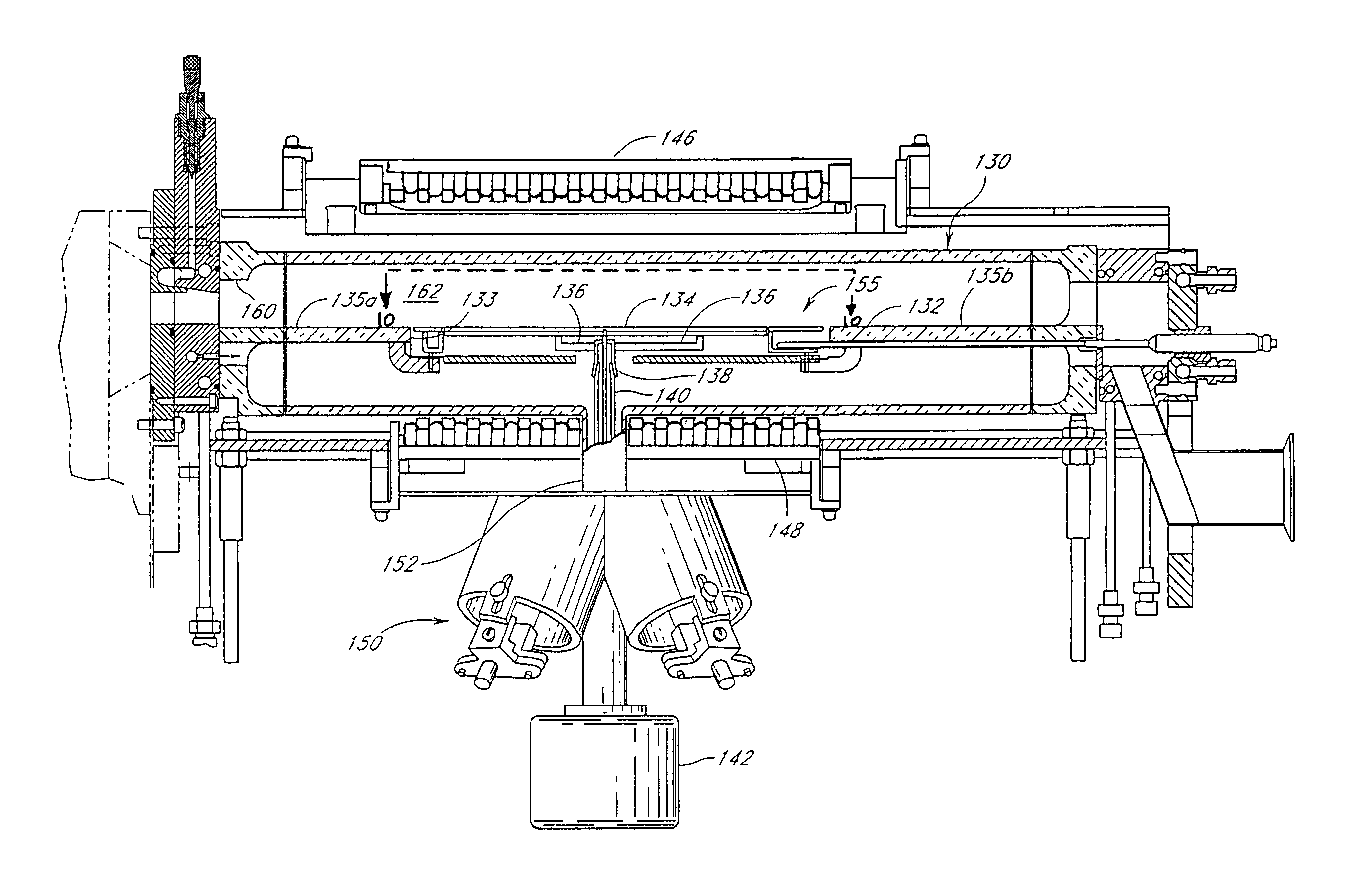
[0011]One aspect is a chemical vapor deposition apparatus that comprises a high temperature processing chamber and a susceptor disposed within the chamber for supporting a wafer to be processed, the susceptor comprising a top surface, a bottom surface, and a perimeter. The apparatus further comprises a plurality of light emitting diodes (LEDs) located on a surface of the chamber, each configured to emit radiant energy towards the top surface, and a controller configured to adjust the radiant energy emitted by at least one of the plurality of LEDs relative to another one of the plurality of LEDs.

[0012]Another aspect is a method of processing a semiconductor in a chamber by applying heat from an array of LED lamps disposed adjacent to the chamber, each LED lamp being configured to emit directional radiant energy towards a substrate in the chamber. The m...


PUM

PropertyMeasurementUnit
heightaaaaaaaaaa
heightaaaaaaaaaa
radiant energyaaaaaaaaaa

Abstract

A reactor chamber is positioned between a top array of LED heat lamps and a bottom array of LED heat lamps. The LED heat lamps forming the top and bottom arrays are individually or controllable in groups such that power output along each array of LED heat lamps can dynamically differ. The LED lamps can be controlled in response to, for example, feedback from chamber sensors, a desired temperature profile, and a failed LED lamp. In this way, the methods and systems described herein can dynamically compensate for operational characteristics of the reactor chamber. In one configuration, the LED heat lamps are arranged in a rectangular pattern. In some configurations, the LED heat lamps are arranged in a circular or a concentric pattern.

Description

RELATED CASES[0001]This application is a continuation of application Ser. No. 10 / 217,230, filed Aug. 9, 2002, now U.S. Pat. No. 6,818,864 and titled LED HEAT LAMP ARRAYS FOR CVD HEATING, which is hereby incorporated by reference in its entirety.BACKGROUND OF THE INVENTION[0002]1. Field of the Invention[0003]The present invention generally relates to heat lamps. More specifically, the present invention relates to heat lamps for improving the temperature uniformity in a field heated by one or more LED heat lamps.[0004]2. Related Art[0005]Chemical vapor deposition (CVD) is a very well known process in the semiconductor industry for forming thin films of materials on substrates, such as silicon wafers. In a CVD process, gaseous molecules of the material to be deposited are supplied to wafers to form a thin film of that material on the wafers by chemical reaction. Such formed thin films may be polycrystalline, amorphous or epitaxial. Typically, CVD processes are conducted at the elevated...

Claims


Application Information

Patent Timeline
Patent Type & Authority Patents(United States)
IPC IPC(8): F27B5/14F26B3/30C23C16/46F27B17/00F27D11/00F27D11/02F27D19/00F27D21/00H01L21/00H01L21/205H01L21/26
CPCC23C16/481H01L21/67115F27B17/0025
Inventor PTAK, JOHN C.
Owner ASM AMERICA INC
Why Eureka
Try Eureka