Devices and systems for electrostatic discharge suppression

a technology of electrostatic discharge and devices, applied in the direction of overvoltage protection resistors, circuit electrostatic discharge protection, emergency protective arrangements for limiting excess voltage/current, etc., can solve the problem of not completely eliminating the risk of damage, more modern devices operating in the higher frequency (ghz and above) using submicron line widths are more susceptible to damage which cannot be overcom

Active Publication Date: 2007-05-15
ELECTRONICS POLYMERS NEWCO
View PDF13 Cites 53 Cited by
  • Summary
  • Abstract
  • Description
  • Claims
  • Application Information

AI Technical Summary

Problems solved by technology

In general, electronic components are damaged following the occurrence of electrical events that cause the transfer of charge from one material to another creating a voltage surge related to voltage potential differences between the two materials.
While such techniques have been effectively used to shield the product from charge and to reduce the generation of charge caused by any movement of product within the container housing the device to be protected, they have not completely eliminated the risk of damage.
Moreover, it is well known that more modern devices operating in the higher frequencies (GHz and above) using submicron line widths are more susceptible to damage which can not be overcome using such methods.
Such prior art protection components, however, suffer from several limitations attributed to the requirement that a substrate or reinforcing layer be used.
Specifically, the use of a substrate adds significantly to the component's overall size and cost.
In addition, the relatively large size and profile of such prior art protection components makes their use impractical in tight spaces where board space is limited.
Moreover, since the substrate material is a primary expense in the manufacture of such components, the use of prior art protection components on a widespread basis can be cost prohibitive.
In addition, the use of prior art ESD protection devices in printed circuit board applications may require an individual device be surface mounted to each component or signal path to be protected which may be cost prohibitive.

Method used


Image

  • Devices and systems for electrostatic discharge suppression
  • Devices and systems for electrostatic discharge suppression
  • Devices and systems for electrostatic discharge suppression

Examples


Embodiment Construction

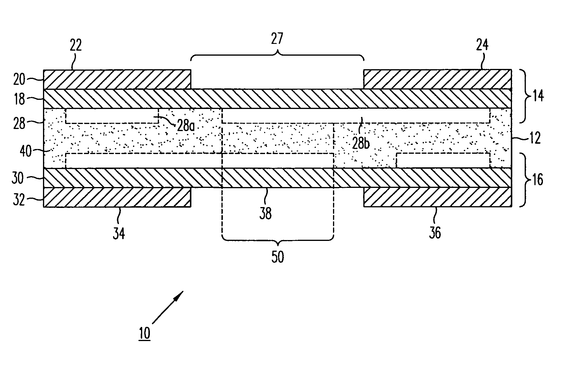
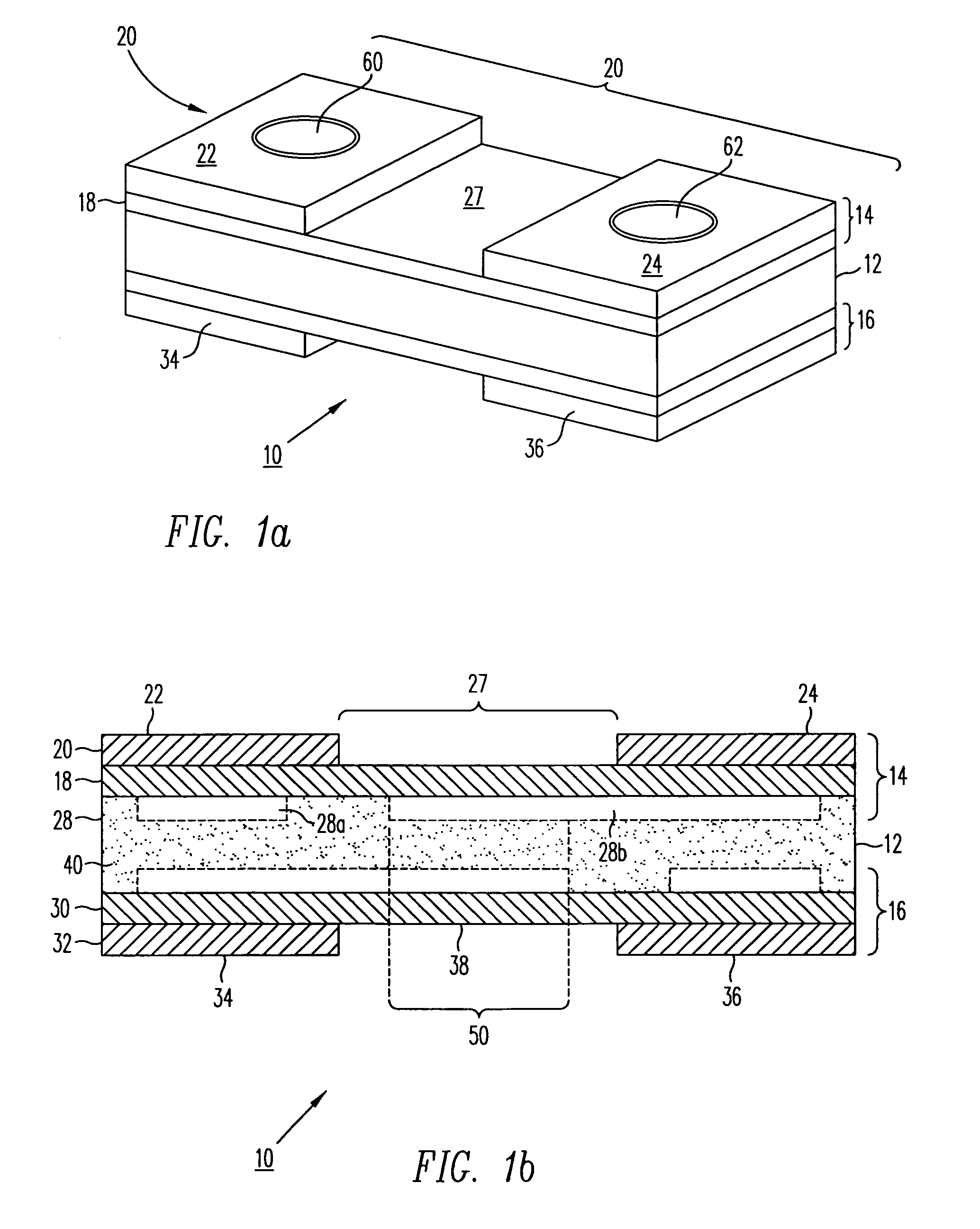
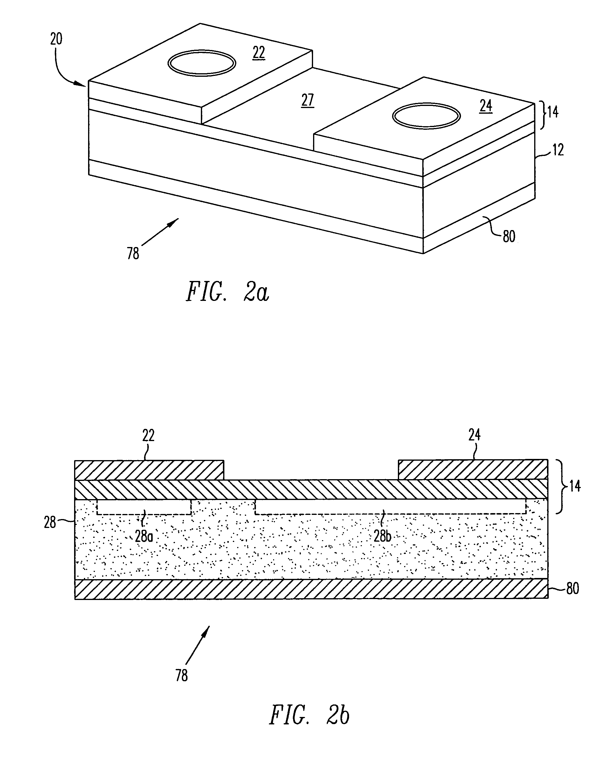
[0020]Referring to FIGS. 1a and 1b, a device 10 for suppressing electrostatic discharge according to one embodiment of the invention is shown consisting of electrostatic discharge reactance layer 12 between first and second multilayer structures 14 and 16. Preferably, the electrostatic discharge reactance layer 12 comprises a polymer-based suppression material such as is described in related application Ser. No. 10 / 366,174 entitled “ESD Protection Devices and Methods of Making Same Using Standard Manufacturing Processes” (the “Related Application”) or a similar material as may be readily obtained in industry from, for example, Electronic Polymers, Inc. and / or other industry sources. The device 10 may be made using standard printed circuit board manufacturing techniques as are well known in the industry and / or as described in the Related Application. Since the performance characteristics of a polymer-based voltage variable material may vary, it is contemplated that device 10 can be u...


PUM


Abstract

A device (10) for suppressing electrostatic discharge comprises first and second multilayer structures (14, 16) surrounding an electrostatic discharge reactance layer (12), the resistance of said electrostatic discharge reactance layer (12) varying in response to the occurrence of an electrostatic discharge signal. Each multilayer structure (14, 16) comprises a barrier layer (18), a terminal layer (20) and an electrode layer (28). Alternatively, a conductive layer (80) can be used instead of a second multilayer structure (16). An ESD suppression device (110) can be embedded in a printed circuit board (122, 210) providing a way to protect board components from harmful ESD events.

Description

CROSS-REFERENCE TO RELATED APPLICATIONS[0001]This application is related to application Ser. No. 10 / 366,174 entitled “ESD Protection Devices and Methods of Making Same Using Standard Manufacturing Processes” filed Feb. 2, 2003, naming common inventor Karen P. Shrier, the entirety of which is incorporated herein by reference.TECHNICAL FIELD[0002]The present invention relates to electronic circuit protection devices and systems including same. More particularly, the invention relates to devices for suppressing electrostatic discharge. Still more particularly, the invention related to a device for ESD suppression comprising first and second multilayer structures surrounding a electrostatic discharge reactance layer, the resistance of which varies in response to the occurrence of an electrostatic discharge signal.BACKGROUND OF THE INVENTION[0003]The problems of static electricity and Electrostatic Discharge (ESD) are well known in the electronics industry. In general, electronic compone...

Claims


Application Information

Patent Timeline
Patent Type & Authority Patents(United States)
IPC IPC(8): H02H9/00
CPCH01C7/10H01C7/13H01C7/18H05K1/0256H05K1/167H05K1/0259H05K1/185H05K3/429H05K2201/0738H01L2924/00014H01L2224/48091H01L2224/48491H01L2224/45099H01L27/04H02H9/00
Inventor SHRIER, KAREN PAMELIA
Owner ELECTRONICS POLYMERS NEWCO
Why Eureka
Try Eureka