Multi-sheet conductive substrates for microelectronic devices and methods for forming such substrates

a technology of conductive substrates and microelectronic devices, applied in the direction of printed circuit aspects, electrical apparatus construction details, printed circuit non-printed electric components association, etc., can solve the problems of circuit board cost and double-sided sheets

Active Publication Date: 2008-04-22
TESSERA INC
View PDF7 Cites 0 Cited by
  • Summary
  • Abstract
  • Description
  • Claims
  • Application Information

AI Technical Summary

Benefits of technology

[0014]The first and second sheets may be movable relative to each other. Movability between the sheets may provide substantial fatigue relief over a temperature range of interest. In the alternative, the first and second sheets may be substantially immobilized relative to each other.

Problems solved by technology

Double-sided sheets, however, may be needed when a single-sided sheet does not have sufficient surface area to contain the conductive regions needed for an intended application.
Via formation, however, can contribute significantly to the cost of circuit boards.

Method used


Image

  • Multi-sheet conductive substrates for microelectronic devices and methods for forming such substrates
  • Multi-sheet conductive substrates for microelectronic devices and methods for forming such substrates
  • Multi-sheet conductive substrates for microelectronic devices and methods for forming such substrates

Examples


Embodiment Construction

[0024]Before describing the present invention in detail, it is to be understood that the invention is not limited to specific microelectronic devices or types of electronic products, as such may vary. It is also to be understood that the terminology used herein is for the purpose of describing particular embodiments only, and is not intended to be limiting.

[0025]As used in this specification and the appended claims, the singular article forms “a,”“an,” and “the” include both singular and plural referents unless the context clearly dictates otherwise. Thus, for example, reference to “a sheet” includes a plurality of posts as well as a single post, reference to “a window” includes an array of windows as well as a single window, reference to “a material” includes a single material as well as a combination of materials, and the like.

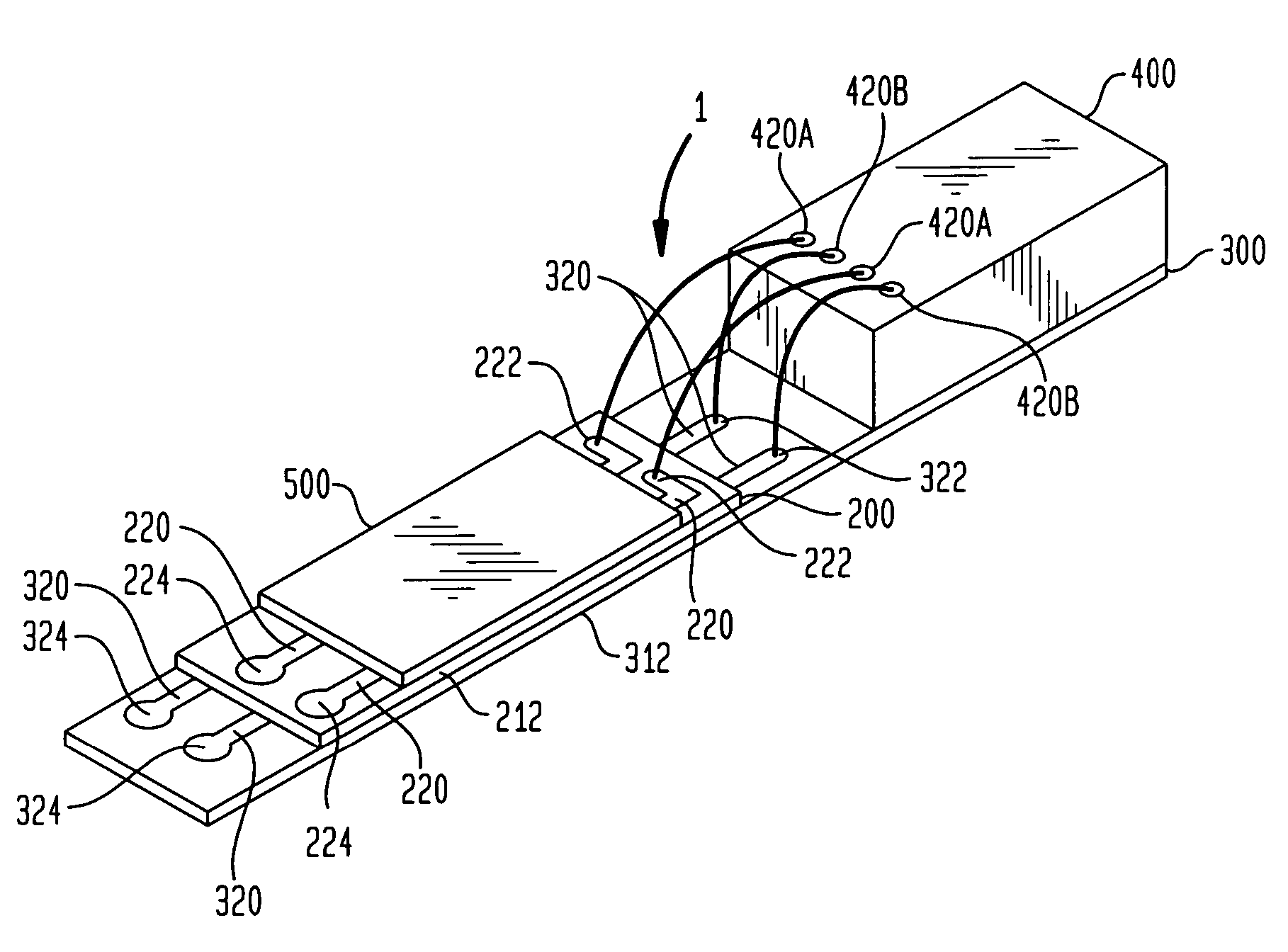
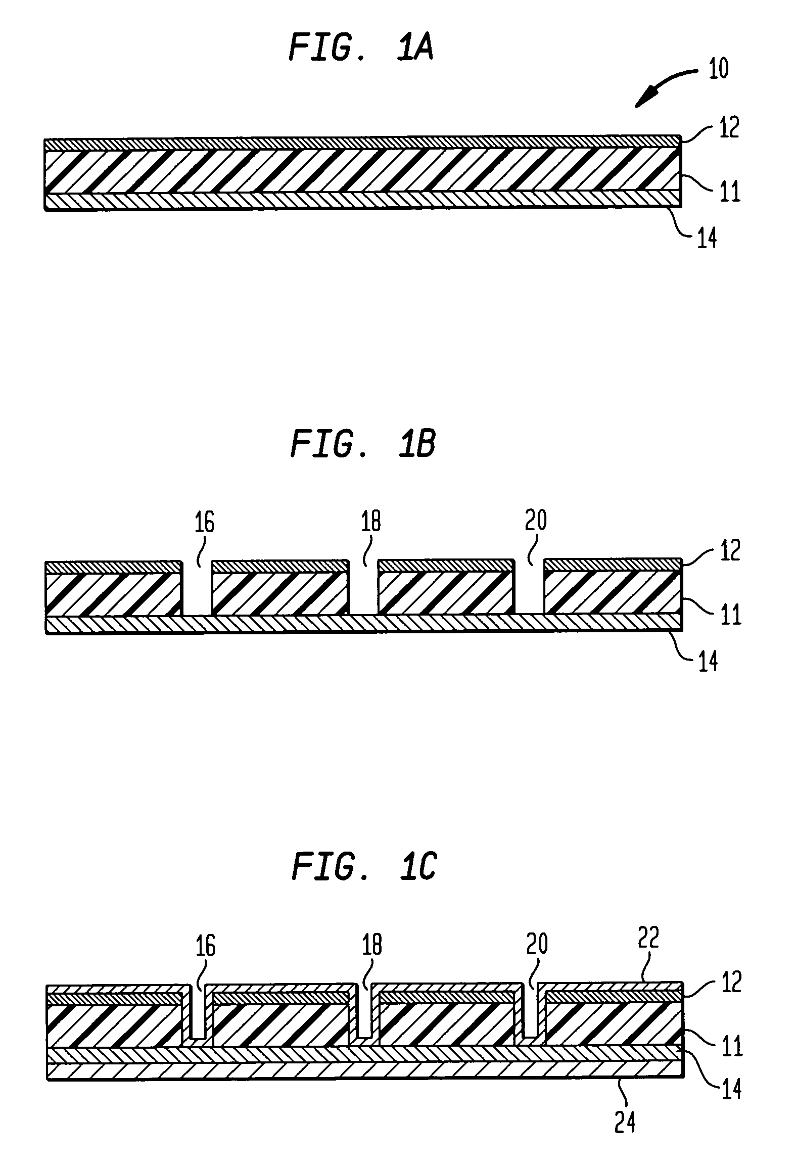
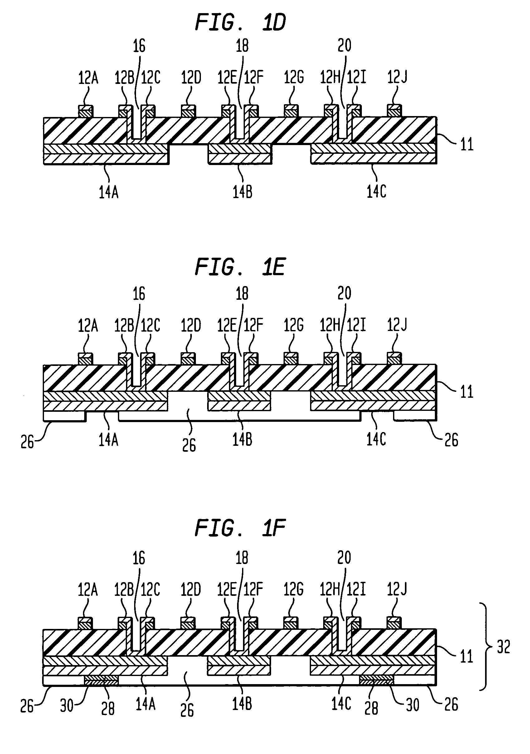
[0026]Certain embodiments of the invention provide substrates for packaging microelectronic devices and to methods for forming such substrates. The inventiv...


PUM


Abstract

A substrate is provided having a plurality of sheets. Each sheet has a first major surface containing a plurality of electrically conductive regions and a second major surface that opposes the first major surface. The sheets are arranged such that the first major surface of a sheet faces the second major surface of another. At least one electrically conductive region of each sheet is partially or fully exposed. At least one electrically conductive region of a sheet is partially or fully covered, e.g., by one or more electrically conductive regions of another sheet. A method for forming such a substrate is also provided.

Description

BACKGROUND OF THE INVENTION[0001]The present invention relates generally to multi-sheet conductive substrates for microelectronic devices. In particular, the invention relates to substrates formed from a plurality of sheets each having electrically conductive regions, wherein at least one sheet has both exposed and covered electrically conductive regions. Also provided are methods for forming multi-sheet conductive substrates.[0002]To increase the portability of electronic products, there is an ongoing effort to miniaturize integrated circuits, processors, and other microelectronic devices such as semiconductor chips. Similarly, as there is a need to increase functionalities of such microelectronic devices, there is an ongoing effort to increase the number of input and output connections in microelectronic devices to other electronic components. As the number of interconnections per microelectronic device increases and the size of microelectronic devices decrease, the number of cont...

Claims


Application Information

Patent Timeline
Patent Type & Authority Patents(United States)
IPC IPC(8): H01L23/02H05K1/00
CPCH01L23/49833H01L23/4985H05K1/112H05K3/4611H05K2201/09472H01L2224/48227H01L2224/49109
Inventor BEROZ, MASUDHABA, BELGACEM
Owner TESSERA INC
Why Eureka
Try Eureka