Dual-plane complementary metal oxide semiconductor

a metal oxide semiconductor, dual-plane technology, applied in the direction of semiconductors, electrical devices, transistors, etc., can solve problems such as performance degradation and/or reliability

Active Publication Date: 2008-04-29
GLOBALFOUNDRIES U S INC
View PDF8 Cites 11 Cited by
  • Summary
  • Abstract
  • Description
  • Claims
  • Application Information

AI Technical Summary

Problems solved by technology

Unfortunately, increased device density in CMOS FETs often results in degradation of performance and / or reliability.

Method used


Image

  • Dual-plane complementary metal oxide semiconductor
  • Dual-plane complementary metal oxide semiconductor
  • Dual-plane complementary metal oxide semiconductor

Examples


Embodiment Construction

[0035]The embodiments of the invention and the various features and advantageous details thereof are explained more fully with reference to the non-limiting embodiments that are illustrated in the accompanying drawings and detailed in the following description. It should be noted that the features illustrated in the drawings are not necessarily drawn to scale. Descriptions of well-known components and processing techniques are omitted so as to not unnecessarily obscure the embodiments of the invention. The examples used herein are intended merely to facilitate an understanding of ways in which the embodiments of the invention may be practiced and to further enable those of skill in the art to practice the embodiments of the invention. Accordingly, the examples should not be construed as limiting the scope of the embodiments of the invention.

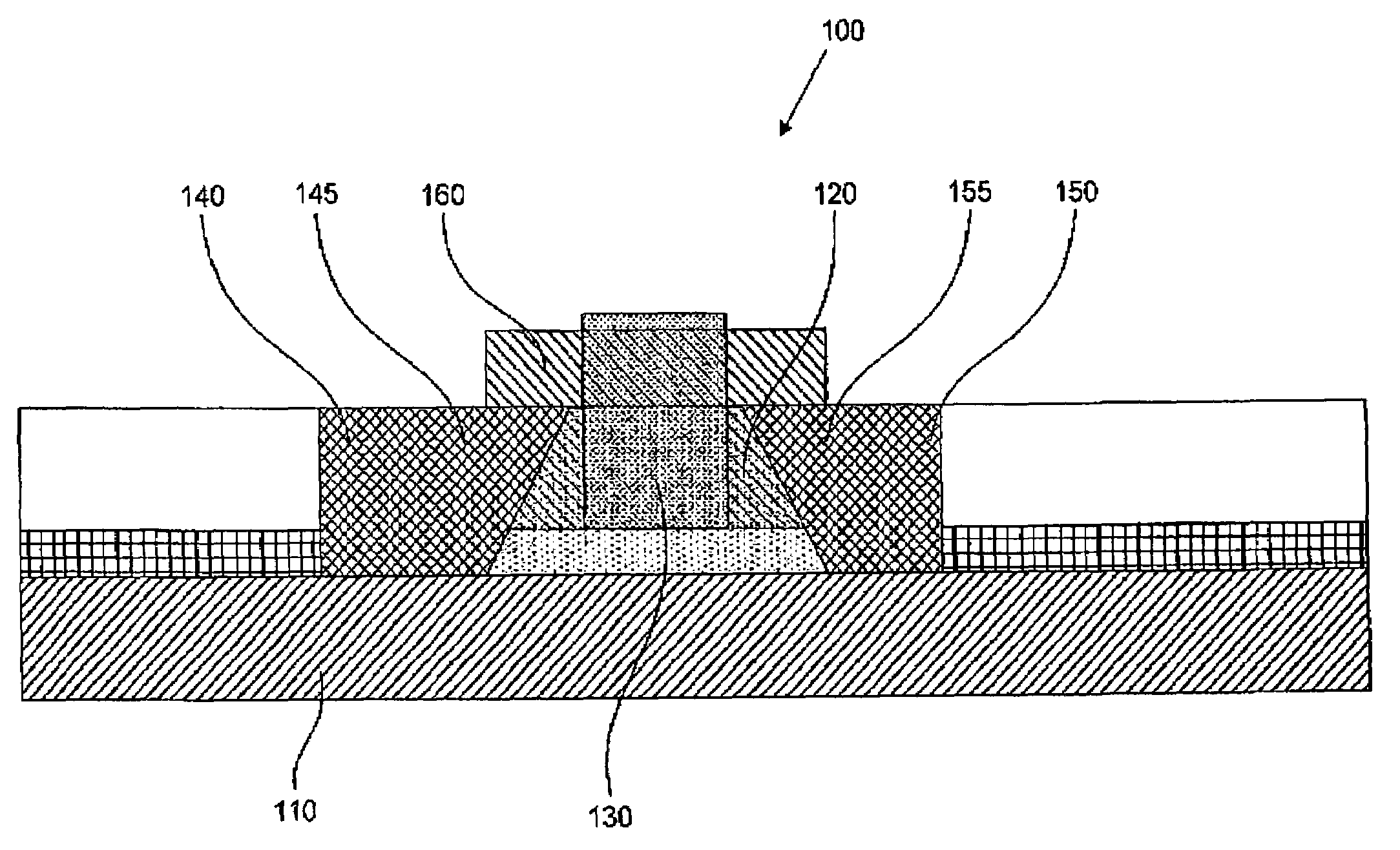
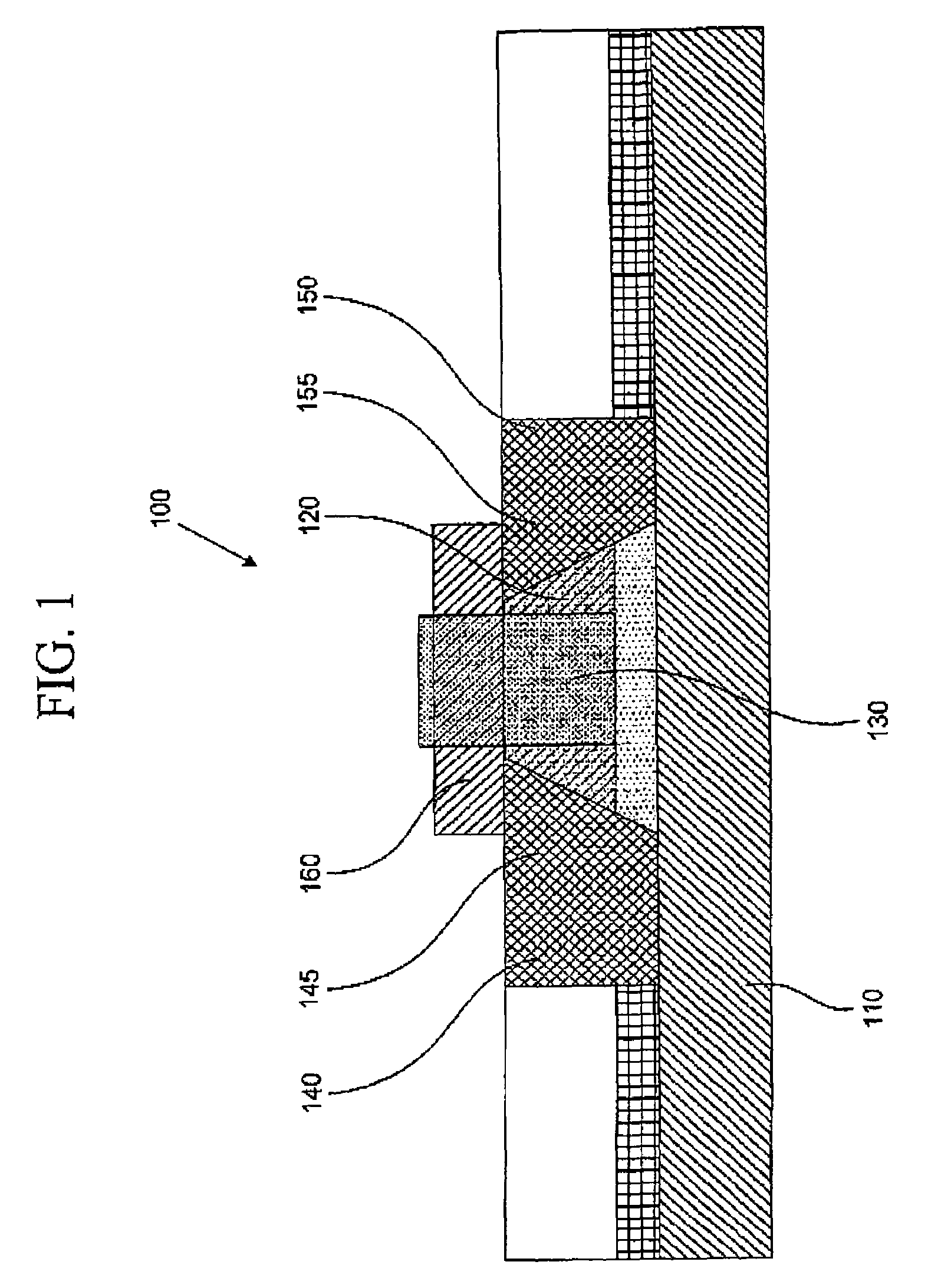
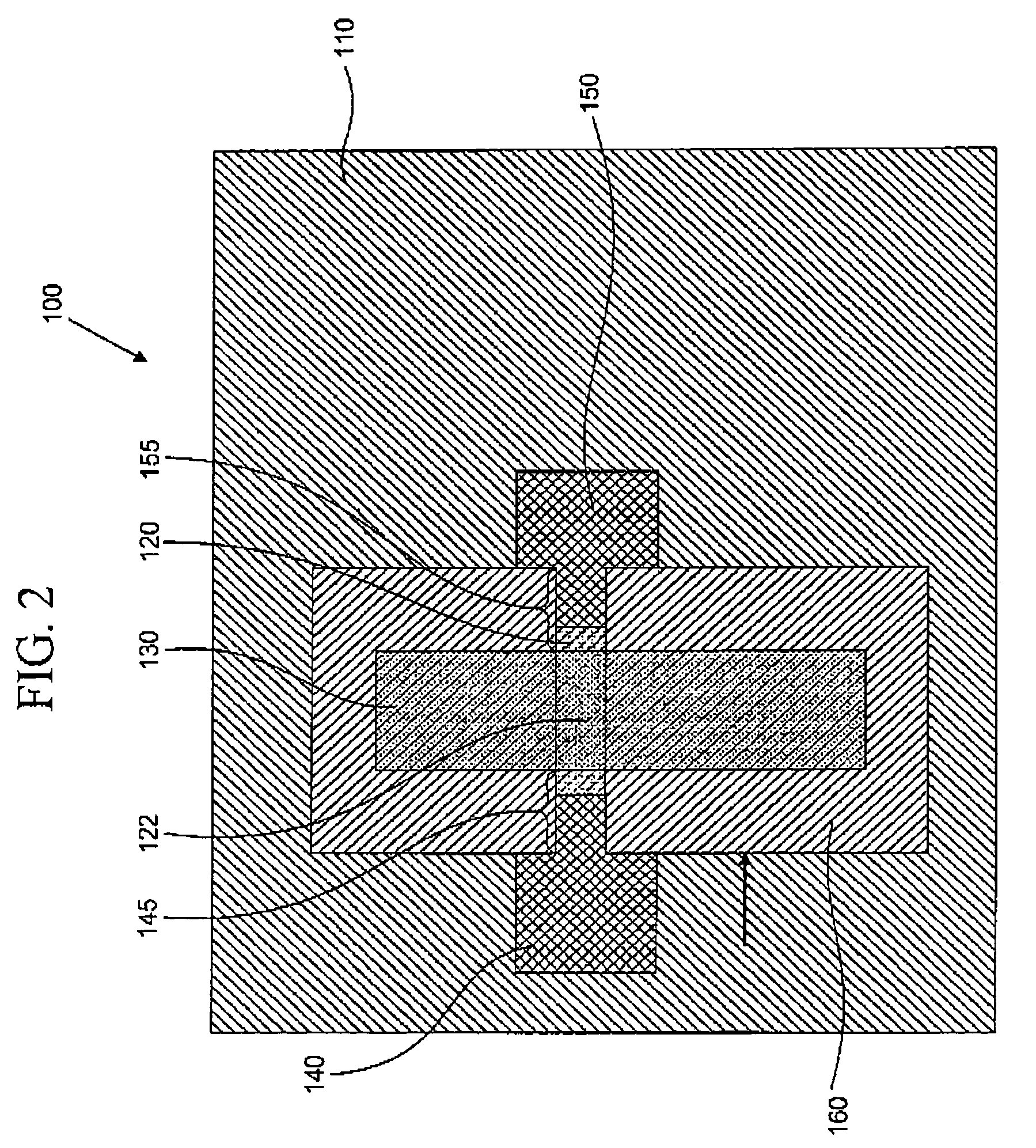
[0036]Embodiments herein present a dual-plane tri-gate with an embedded silicon-germanium source and drain on pFET and tensile nitride overlayer...


PUM


Abstract

Embodiments herein present a device, method, etc. for a dual-plane complementary metal oxide semiconductor. The device comprises a fin-type transistor on a bulk silicon substrate. The fin-type transistor comprises outer fin regions and a center semiconductor fin region, wherein the center fin region has a {110} crystalline oriented channel surface. The outer fin regions comprise a strain inducing material that stresses the center semiconductor fin region. The strain inducing material contacts the bulk silicon substrate, wherein the strain inducing material comprises germanium and / or carbon. Further, the fin-type transistor comprises a thick oxide member on a top face thereof. The fin-type transistor also comprises a first transistor on a first crystalline oriented surface, wherein the device further comprises a second transistor on a second crystalline oriented surface that differs from the first crystalline oriented surface.

Description

BACKGROUND[0001]1. Field of the Invention[0002]Embodiments herein present a device, method, etc. for a dual-plane complementary metal oxide semiconductor (CMOS).[0003]2. Description of the Related Art[0004]The need to remain cost and performance competitive in the production of semiconductor devices has caused continually increasing device density in integrated circuits. To facilitate the increase in device density, new technologies are constantly needed to allow the feature size of these semiconductor devices to be reduced.[0005]The push for ever-increasing device densities is particularly strong in CMOS technologies, such as in the design and fabrication of field effect transistors (FETs). FETs are used in almost all types of integrated circuit design (i.e., microprocessors, memory, etc.). Unfortunately, increased device density in CMOS FETs often results in degradation of performance and / or reliability.[0006]One type of FET that has been proposed to facilitate increased device de...

Claims


Application Information

Patent Timeline
Patent Type & Authority Patents(United States)
IPC IPC(8): H01L29/76
CPCH01L21/823807H01L21/823828H01L29/7842H01L29/7848H01L29/785H01L29/78687
Inventor ANDERSON, BRENT A.NOWAK, EDWARD J.
Owner GLOBALFOUNDRIES U S INC
Why Eureka
Try Eureka