Low latency switch architecture for high-performance packet-switched networks

a switch architecture and packet-switching network technology, applied in the field of low-latency switch architecture, can solve the problems of limiting the size of the switching fabric that can be implemented on a single chip, switch architectures using crossbars are simple to build, and still represent bottlenecks in high-performance low-latency networks. , to achieve the effect of low latency

Inactive Publication Date: 2008-10-07
THE UNITED STATES OF AMERICA AS REPRESENTED BY THE SECRETARY OF THE NAVY
View PDF3 Cites 38 Cited by
  • Summary
  • Abstract
  • Description
  • Claims
  • Application Information

AI Technical Summary

Problems solved by technology

However, switches still represent a bottleneck in high-performance low-latency networks.
Switch architectures that used crossbars are simple to build, but are not scalable and suffer from contention when several inputs try to connect to a single output.
In this situation, the buffer memory requires a much larger amount of real estate than the switching array itself, and combining these components on the same ASIC (Application Specific Integrated Circuit) or FPGA (Field Programmable Gate Array) would limit the size of the switching fabric that can be implemented on a single chip.
In memory management, fine-tuned switch architectures can attain high throughput, but these require either complex scheduling algorithms, which are difficult to realize in hardware or memories working at speeds greater than the link rate.
Most of these high speed switch architectures require large amounts of buffer space or high-speed memory access.
However the performance will be limited by the access time to the memory, and highly efficient memory access control is required as well.
Internal memory is faster than external memory but expensive in terms of chip real estate and limited in size.
One of the logic designer's biggest challenge is effectively utilizing the memory present within an ASIC (Application Specific Integrated Circuit) or FPGA (Field Programmable Gate Array).
In addition to being a limited resource, memory blocks internal to the chip are not capable of running at speeds required by the shared medium switches and other fast packet switch architectures, which require a minimum speed of twice the link rate.

Method used


Image

  • Low latency switch architecture for high-performance packet-switched networks
  • Low latency switch architecture for high-performance packet-switched networks
  • Low latency switch architecture for high-performance packet-switched networks

Examples


Embodiment Construction

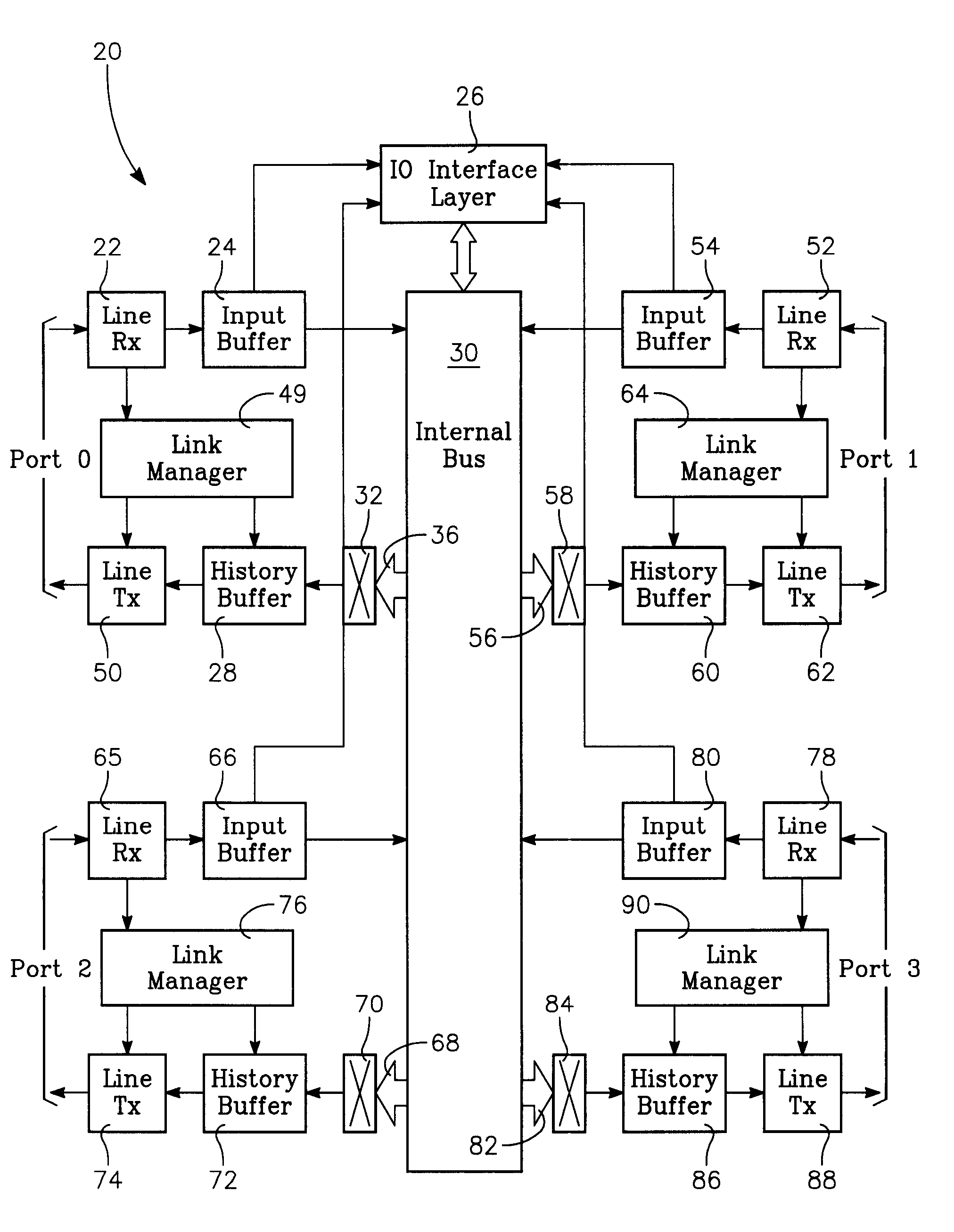
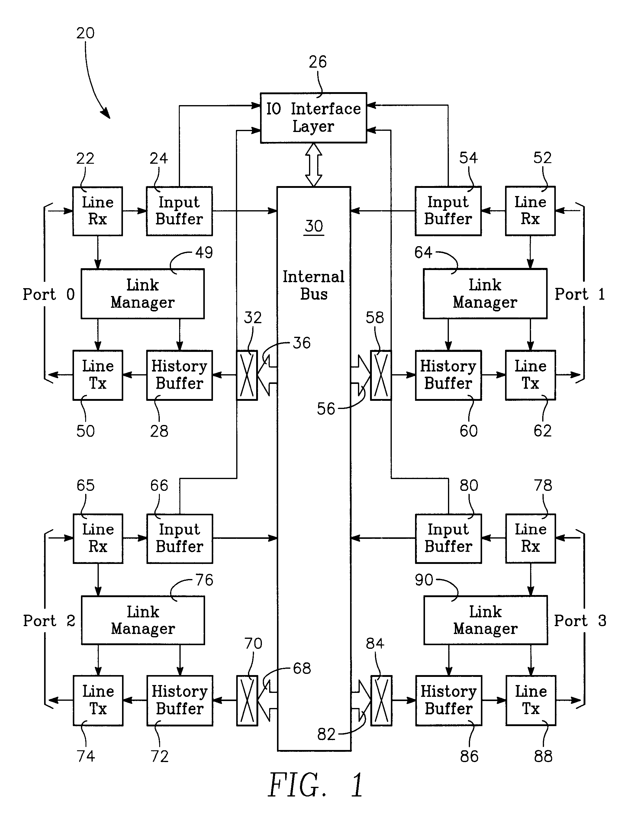
[0038]The present invention relates to low latency switch architecture, and more specifically, to a low latency switch architecture for high performance packet-switched networks. The switch architecture of the present invention comprises a combination of input buffers capable of avoiding head-of-line blocking at the input ports for the switch and also allows for a packet to be passed the switch fabric on to the output port provided there is a free buffer at the output port. The switch architecture also includes an internal switch interconnect capable of allowing different input ports to access a single output simultaneously.

[0039]Referring to FIGS. 1 and 2, FIG. 1 illustrates the present switch architecture and is identified generally by the reference numeral 20. Switch architecture 20 avoids head-of-line blocking at the input ports for Port 0, Port 1, Port 2 and Port 3, and allows any data packet to be passed through the switch architecture 20 to an output port regardless of how ma...


PUM


Abstract

A low latency switch architecture for high performance packet-switched networks which is a combination of input buffers capable of avoiding head-of-line blocking and an internal switch interconnect capable of allowing different input ports to access a single output simultaneously.

Description

[0001]This application claims the benefit of U.S. Provisional Application No. 60 / 605,251, filed Aug. 23, 2004.STATEMENT REGARDING FEDERALLY SPONSORED RESEARCH OR DEVELOPMENT[0002]The invention described herein may be manufactured and used by or for the government of the United States of America for governmental purposes without the payment of any royalties thereon or therefor.FIELD OF THE INVENTION[0003]The present invention relates generally to low latency switch architecture, and more specifically, to a low-latency switch architecture for high-performance computing and signal processing networks.BACKGROUND OF THE INVENTION[0004]Switches are an important factor in determining performance of any modern interconnect network designed for high-performance computing and signal processing. Over the past years a number of switch architectures have made their mark in packet-switched applications. However, switches still represent a bottleneck in high-performance low-latency networks.[0005]...

Claims


Application Information

Patent Timeline
Patent Type & Authority Patents(United States)
IPC IPC(8): H04L12/28
CPCH04L49/3018H04L49/102H04L49/3009
Inventor ROSEN, WARRENSUKHTANKAR, SATYENLACHENMAIER, RALPH N.
Owner THE UNITED STATES OF AMERICA AS REPRESENTED BY THE SECRETARY OF THE NAVY
Why Eureka
Try Eureka