

Method for manufacturing a lower substrate of a liquid crystal display device
a liquid crystal display and substrate technology, applied in the testing/measurement of individual semiconductor devices, semiconductor/solid-state devices, instruments, etc., can solve the problems of light leakage and reduce the yield throughout, so as to reduce the number of masks or the manufacturing process, the effect of simplifying the manufacturing process and reducing the number of masks
- Summary
- Abstract
- Description
- Claims
- Application Information
AI Technical Summary
Benefits of technology
Problems solved by technology
Method used
Image

Examples
embodiment 1
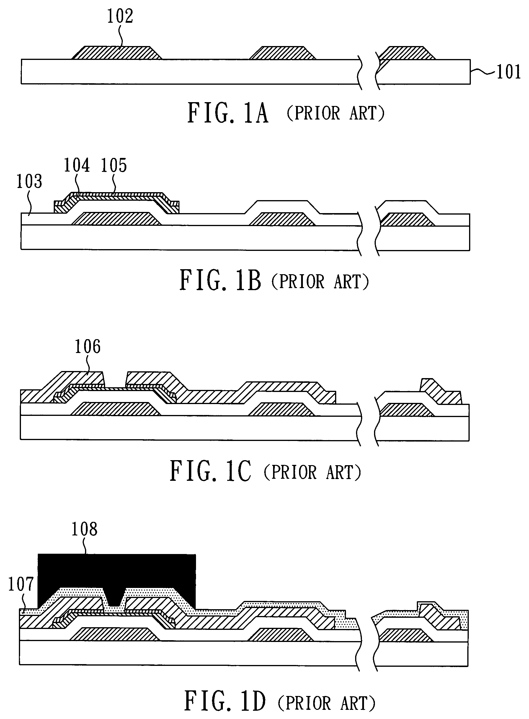
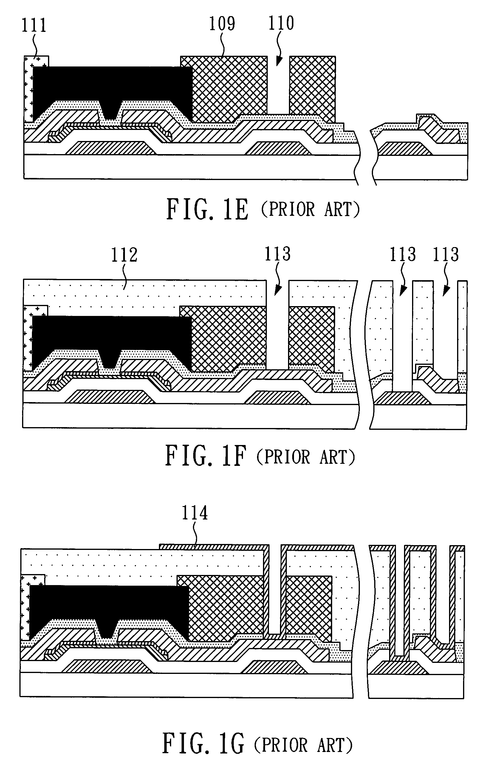
[0040]The present embodiment uses a photosensitive insulating layer as a passivation layer or an overcoat of the TFT so as to reduce the photographic steps by one.
[0041]Please refer to FIGS. 2A to 2G, wherein cross-sectional views illustrate the process for manufacturing a lower substrate of an LCD device of the present embodiment.
[0042]A first metal layer (not shown) is first formed on a substrate 201 by sputtering, and a gate 202 in the thin film transistor region A, a lower electrode 203 in the auxiliary capacitance region, and a terminal line 204 in the connecting terminal region are defined. Subsequently, a gate insulating layer 205 (SiNx) is formed by PECVD. Then, a semiconductor layer 208 (a-Si) and an ohmic contact layer 222 (n+Si) are formed by depositing, and then the semiconductor layer 208 and the ohmic contact layer 222 are patterned to form an active region. Subsequently, a second metal layer (not shown) of a Ti / Al / Ti multi-layered structure is formed by sputtering, an...
embodiment 2
[0049]The present embodiment uses a photosensitive insulating layer as a passivation layer or an overcoat of the TFT to reduce the photographic steps by one. In addition, the present embodiment improves the method of Embodiment 1 to omit the dry-etching process for a contact hole in the connecting terminal region C, and to inhibit the issues of reduced thickness of the black matrix and the color filter layer resulting from ion impact.
[0050]Please refer to FIGS. 3A to 3G, wherein cross-sectional views illustrate the process for manufacturing a lower substrate of an LCD device of the present embodiment.
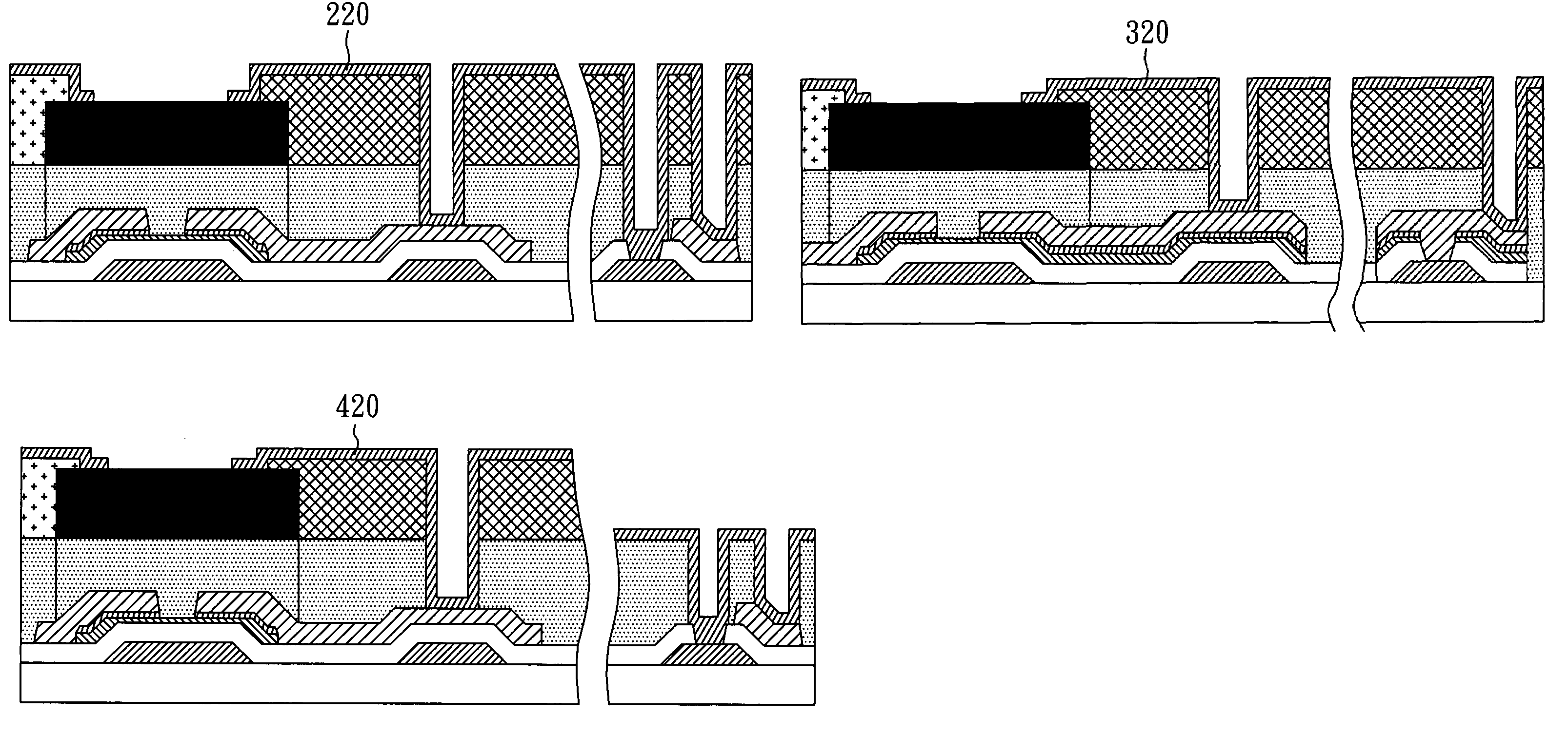
[0051]A first metal layer (not shown) is first formed on a substrate 301 by sputtering, and a gate 302 in the thin film transistor region A, a lower electrode 303 in the auxiliary capacitance region B, and a terminal line 304 in the connecting terminal region C are defined. As shown in FIG. 3B, a gate insulating layer 305 (SiNx) is formed by PECVD. Then, a semiconductor layer 308 (a-Si)...
embodiment 3
[0057]The present embodiment uses a photosensitive insulating layer as a passivation layer or an overcoat of the TFT to reduce the photographic steps by one. In addition, the present embodiment improves the method of Embodiment 1 to further reduce the photographic steps by two via ink-jet printing so as to form three color filter layers of different colors. The manufacturing steps and the manufacturing cost are reduced due to reducing omitting the number of steps in photosensitive insulating layer coating.
[0058]Please refer to FIGS. 4A to 4F, wherein cross-sectional views illustrate the process for manufacturing a lower substrate of an LCD device of the present embodiment.
[0059]A lower substrate 400 of an LCD device is provided, as shown in FIG. 4A. The process for forming the lower substrate 400 is the same as the process for forming the structure of FIG. 2A of Embodiment 1.
[0060]Subsequently, a first negative photosensitive insulating layer 413 is formed by coating and then by pre...
PUM
 Abstract
Description
Claims
Application Information