Evaluation unit in an integrated circuit

a technology of integrated circuits and evaluation units, applied in the field of integrated circuits, can solve the problems of high manufacturing cost and process complexity, and achieve the effects of improving memory modules, improving computer performance, and improving memory devices

Active Publication Date: 2009-09-08
POLARIS INNOVATIONS LTD
View PDF6 Cites 0 Cited by
  • Summary
  • Abstract
  • Description
  • Claims
  • Application Information

AI Technical Summary

Benefits of technology

[0008]Various embodiments of the present invention may provide particular advantages for an improved integrated circuit, for an improved memory device, for an improved memory module, for an improved computer system, and for an improved method of operating a memory device.

Problems solved by technology

While the storage capacity of modern memory devices is steadily increased, also the manufacturing costs of a modern memory device may be an important factor for its economic success.
Since conventional manufacturing processes may still require different packaging, chip carriers, and / or bonding, manufacturing costs and process complexity may be still too high for an economic provision of modern memory devices with options and product variations.

Method used


Image

  • Evaluation unit in an integrated circuit
  • Evaluation unit in an integrated circuit
  • Evaluation unit in an integrated circuit

Examples


first embodiment

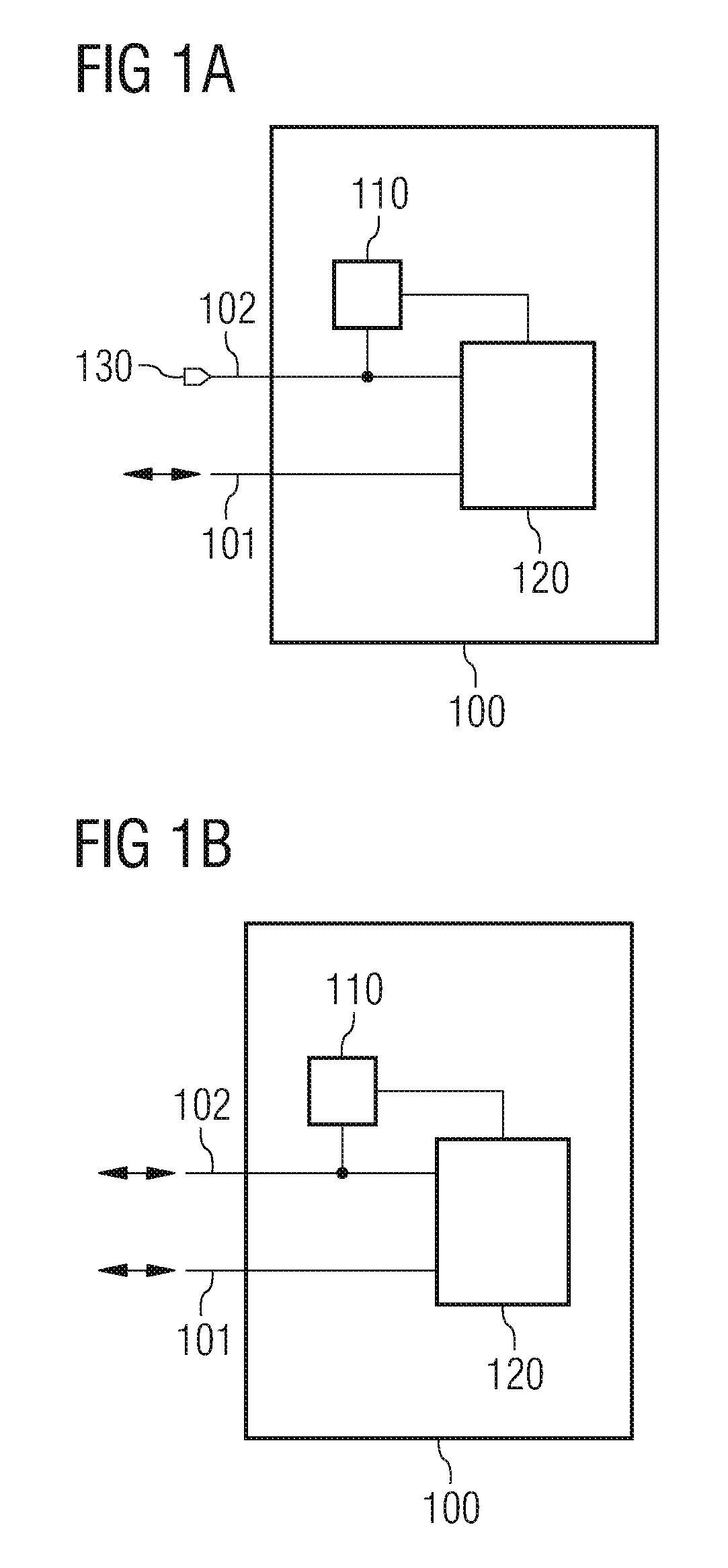
[0023]FIG. 1A shows a schematic view of an integrated circuit 100 according to the present invention. The integrated circuit 100 comprises an evaluation unit 110 and a switching unit 120. The integrated circuit 100 further comprises a first terminal 101 and a second terminal 102.

[0024]The integrated circuit 100 exchanges signals via the first terminal 101 and the second terminal 102. The terminals 101, 102 may comprise a single signal line or a port with more than one signal line for receiving and / or transmitting signals. According to this embodiment of the present invention, the second terminal 102 of the integrated circuit 100 is coupled to a signal source, for example a voltage source 130 as shown in FIG. 1A. For example, upon initialization or power up, the evaluation unit 110 determines a voltage level being applied to the second terminal 102 by the voltage source 130. In case the determined voltage corresponds to a control voltage, the evaluation unit 110 instructs the switchi...

second embodiment

[0025]FIG. 1B shows a schematic view of the integrated circuit 100 according to the present invention. According to this embodiment, the integrated circuit 100, comprising the evaluation unit 110, the switching unit 120, the first terminal 101, and the second terminal 102, is supposed to exchange signals via both terminals 101, 102. In this case, the second terminal 102 may be coupled to other entities of a superordinate circuitry. However, it may be connected such that the evaluation unit 110 does not determine a voltage at the second terminal 102 that corresponds to said control voltage, as described in conjunction with FIG. 1A in which the second terminal 102 is coupled to the control voltage source 130. According to this embodiment, the evaluation unit 110 instructs the switching unit 120 such that both terminals 101, 102 are used for signal exchange.

third embodiment

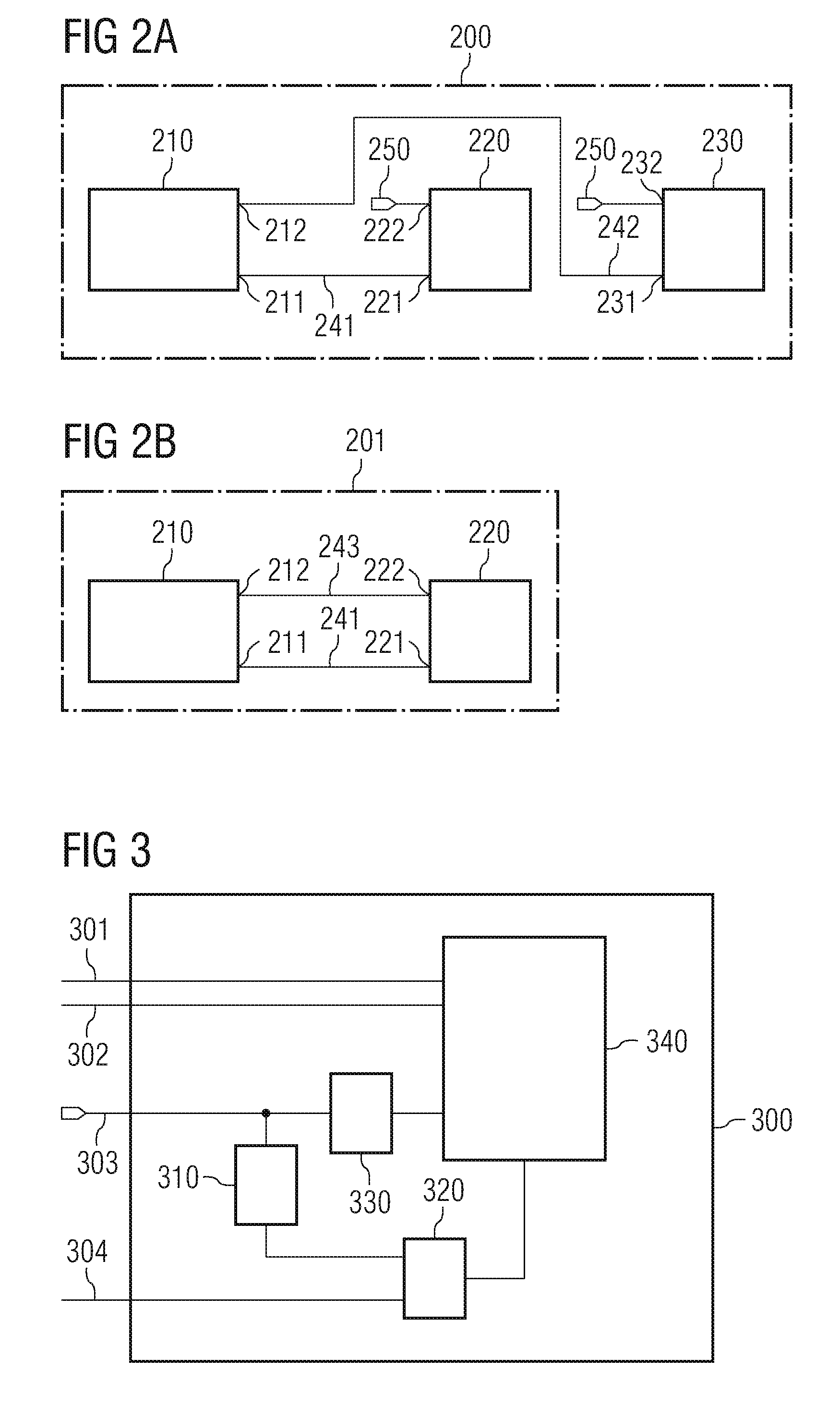
[0026]FIG. 2A shows a schematic view of a first computer system 200 according to the present invention. The computer system 200 comprises a first device 210, a second device 220, and a third device 230. A first terminal 211 of the first device 210 is coupled to a first terminal 221 of the second device 220 via a first signal line 241. A second terminal 212 of the first device 210 is coupled to a first terminal 231 of the third device 230 via a second signal line 242. A second terminal 222 of the second device 220 and a second terminal 232 of the third device 230 are coupled to a voltage source 250.

[0027]According to this embodiment of the present invention, the first device 210 may exchange signals with the second device 220 and the third device 230 via the signal lines 241, 242. The devices 220, 230, being, for example, integrated circuits 100 as described in conjunction with FIG. 1A, only employ their first terminal 221, 231 respectively for signal exchange. The application of a c...


PUM


Abstract

An integrated circuit comprising a first terminal for exchanging signals; an evaluation unit coupled to the first terminal, the evaluation unit evaluating a signal level applied to the first terminal to determine whether or not the signal level corresponds to a predetermined signal level; and a switching unit coupled to the first terminal and to the evaluation unit, the switching unit admitting signal exchange via the first terminal if the evaluation unit does not determine the predetermined signal level, the switching unit cutting off signal exchange via the first terminal if the evaluation unit determines the predetermined signal level.

Description

BACKGROUND OF THE INVENTION[0001]1. Field of the Invention[0002]The present invention relates to an integrated circuit, a memory device, a memory module, and a computer system. The present invention further relates to a method of operating a memory device.[0003]2. Description of the Related Art[0004]Demands imposed on large scale integrated circuits are constantly increasing. In the case of memory devices, said demands mainly translate into speed and storage capacity. As far as high speed memory devices are concerned, the computer industry has established the so-called DRAM (Dynamic Random Access Memory) as economic means for high-speed and high-capacity data storage.[0005]Although a DRAM requires a continuous refreshing of the stored information, speed and information density, combined with a relatively low cost, have put the DRAM in a pivotal position in the field of information technology. Almost every modern computer system, ranging, for example, from PDAs over notebook computer...

Claims


Application Information

Patent Timeline
Patent Type & Authority Patents(United States)
IPC IPC(8): G06F12/00G06F13/00G06F13/42
CPCG11C5/04
Inventor HEIN, THOMASNYGREN, AARON JOHNKHO, REX
Owner POLARIS INNOVATIONS LTD
Why Eureka
Try Eureka