Phase shift adjusting method and circuit

a phase shift and adjustment method technology, applied in the field of phase shift adjustment method and circuit, can solve the problems of increasing the error rate in data detection at the receiver, unable to provide any mechanism for present or already projected future dram standards, and serious challenge in timing of signals relative to the clock. , to achieve the effect of improving memory controller and improving memory devi

Inactive Publication Date: 2010-11-16
POLARIS INNOVATIONS LTD
View PDF13 Cites 30 Cited by
  • Summary
  • Abstract
  • Description
  • Claims
  • Application Information

AI Technical Summary

Benefits of technology

[0008]The present invention provides advantages for an improved method of adjusting a phase shift between a data signal and a clock signal, an improved memory controller and an improved memory device.

Problems solved by technology

With data rates like these, the timing of the signals relative to the clock is a serious challenge.
Any unforeseen delay of a data signal or of a clock signal drastically increases the error rate in the data detection at the receiver.
However, neither present nor already projected future DRAM standards provide any mechanism for returning information about the phase alignment at the receiving memory device to the memory controller.
However, the circuitry for this solution is quite complex, in particular the computations are time consuming and require special circuitry in the memory controller.
Thereby the costs of production of the memory controller are increased.

Method used


Image

  • Phase shift adjusting method and circuit
  • Phase shift adjusting method and circuit
  • Phase shift adjusting method and circuit

Examples


Embodiment Construction

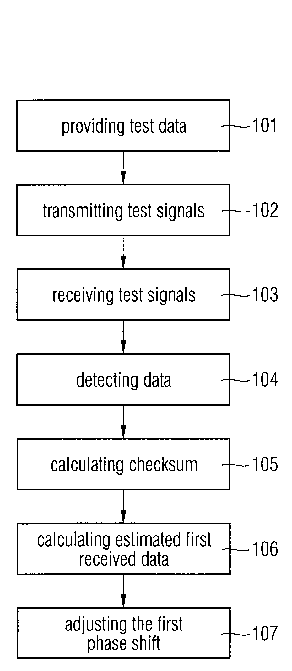
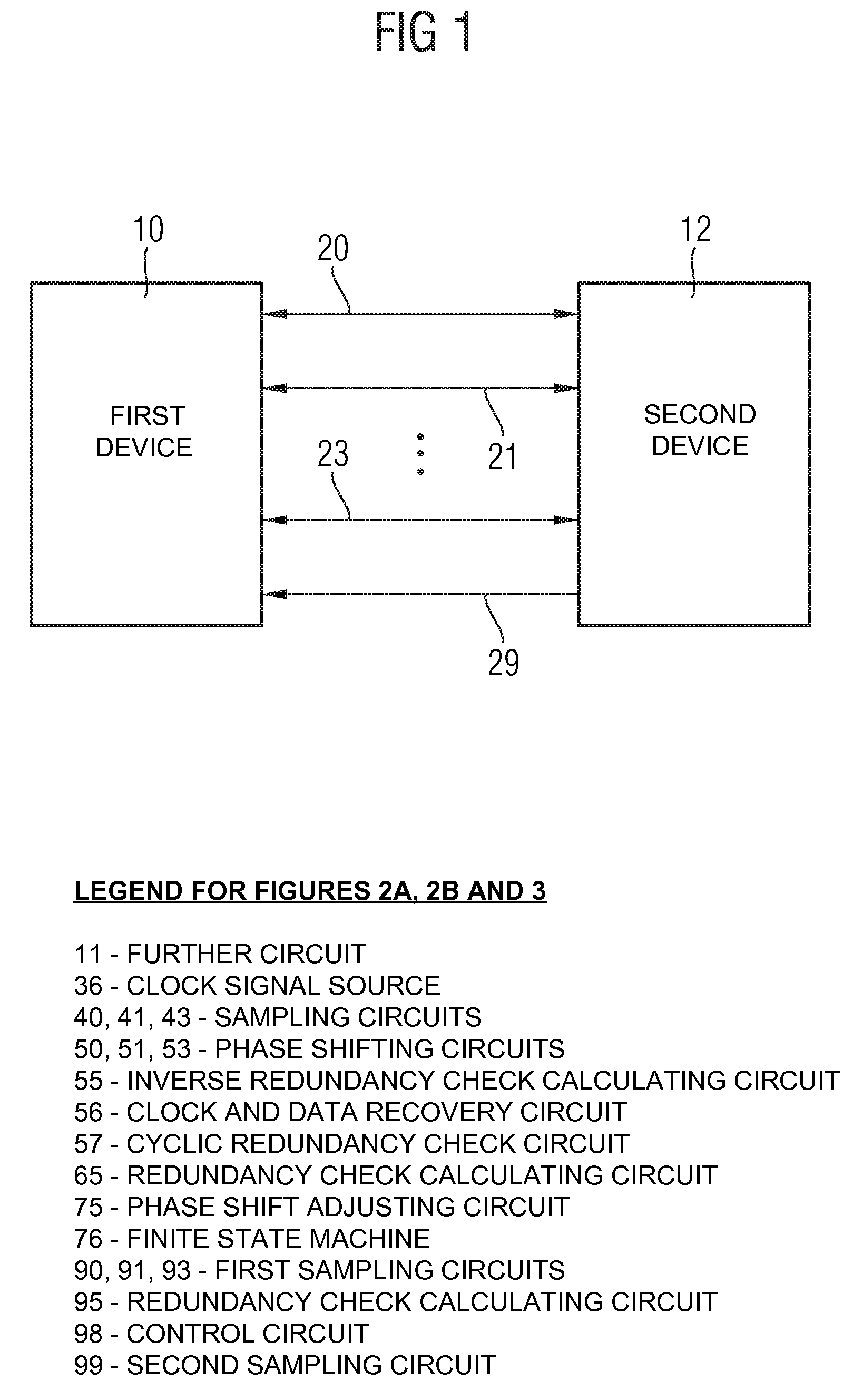
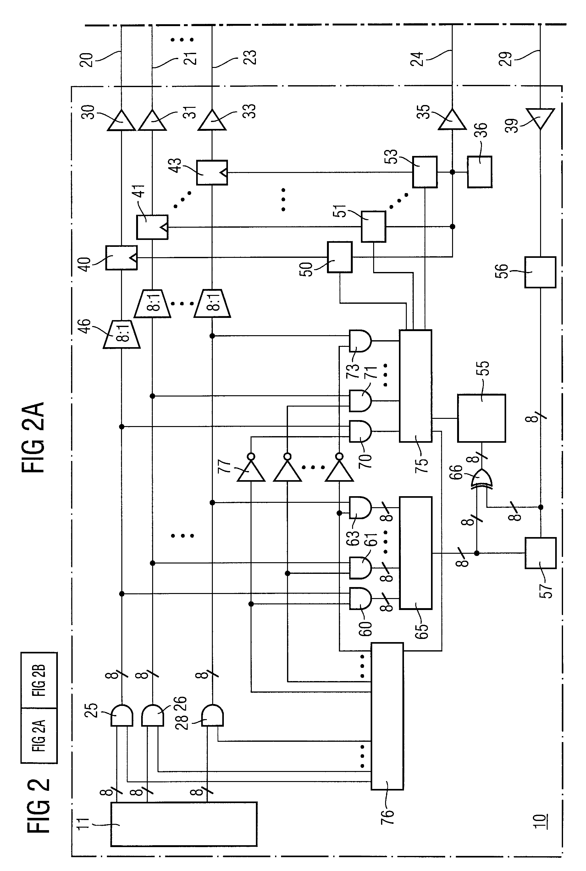
[0018]FIG. 1 is a schematic flow chart of a first device 10 and a second device 12 wherein both the first and the second devices 10, 12 are preferably microelectronic devices like memory controllers or memory devices. The first and second devices 10, 12 are connected to each other via a plurality of data signal lines 20, 21, 23 and an error detecting code signal line 29. The data signal lines 20, 21, 23 are configured to transmit data signals from the first device 10 to the second device 12 and / or from the second device 12 to the first device 10. The error detecting code signal line is configured to transmit an error detecting code signal from the second device 12 to the first device 10. The first and second devices 10, 12 may be connected to each other via a number of further data, address, command or other signal lines which are not displayed in FIG. 1. In particular, the first and second devices 10, 12 are preferably connected via a clock signal line transmitting a clock signal f...


PUM


Abstract

Method and system of adjusting a first phase shift between a first data signal and a clock signal at a sending device. First and second test signals representing first and second test data, respectively, are transmitted to a receiving device. The test signals have respective phase shifts relative to the clock signal. An error detection code is calculated from first and second received data carried by the transmitted signals. The error detection code is transmitted from the receiving device to the sending device. An estimated first received data is calculated from the error detection code, wherein the estimated first received data are calculated under the assumption that the second received data are identical to the second test data. The first phase shift is adjusted on the basis of a comparison of the estimated first received data and the first test data.

Description

BACKGROUND OF THE INVENTION[0001]1. Field of the Invention[0002]The present invention refers to methods of adjusting a phase shift between a data signal and a clock signal, and to devices providing an adjustment of a phase shift between a data signal and a clock signal.[0003]2. Description of the Related Art[0004]In graphics applications and in other applications the data rate of the exchange of data between a memory controller and a memory device is increased more and more. According to the GDDR5-standard, the data rate will be up to 4 Gbit / s / pin or even 5 Gbit / s / pin. With data rates like these, the timing of the signals relative to the clock is a serious challenge. Any unforeseen delay of a data signal or of a clock signal drastically increases the error rate in the data detection at the receiver.[0005]An automatic adjustment mechanism could reduce the static mismatches between the propagation paths of each single data signal and a clock signal. Thereby, voltage and temperature de...

Claims


Application Information

Patent Timeline
Patent Type & Authority Patents(United States)
IPC IPC(8): G06F11/00H04L12/43
CPCG06F11/1004H04L7/0037G11C7/1078G11C7/1084G11C7/22G11C11/4076G11C11/4093G11C29/02G11C29/023G11C29/025G11C29/028G11C29/50012H04L7/0091H04L7/048H03M13/33G01R31/31725G06F11/073G06F1/10G06F11/18G06F11/186G01R31/31937G06F11/263G11C2207/2254H04L7/0008H04L7/02H04L1/00
Inventor SCHUMACHER, OTTOMAIER, MARTINHEIN, THOMASNYGREN, AARON JOHN
Owner POLARIS INNOVATIONS LTD
Why Eureka
Try Eureka