Integrated circuit and memory device

Inactive Publication Date: 2008-10-23
QIMONDA
View PDF4 Cites 0 Cited by
  • Summary
  • Abstract
  • Description
  • Claims
  • Application Information

AI Technical Summary

Benefits of technology

[0005]Various embodiments of the present invention may provide particular advantages for an improved memory device, an improved memory module, an improved integrated device, an improved circuit system, or an improved method of operating an integrated device.

Problems solved by technology

While the storage capacity of modern memory devices is steadily increased, also the manufacturing costs of a modern memory device may be an important factor for its economic success.

Method used


Image

  • Integrated circuit and memory device
  • Integrated circuit and memory device
  • Integrated circuit and memory device

Examples


first embodiment

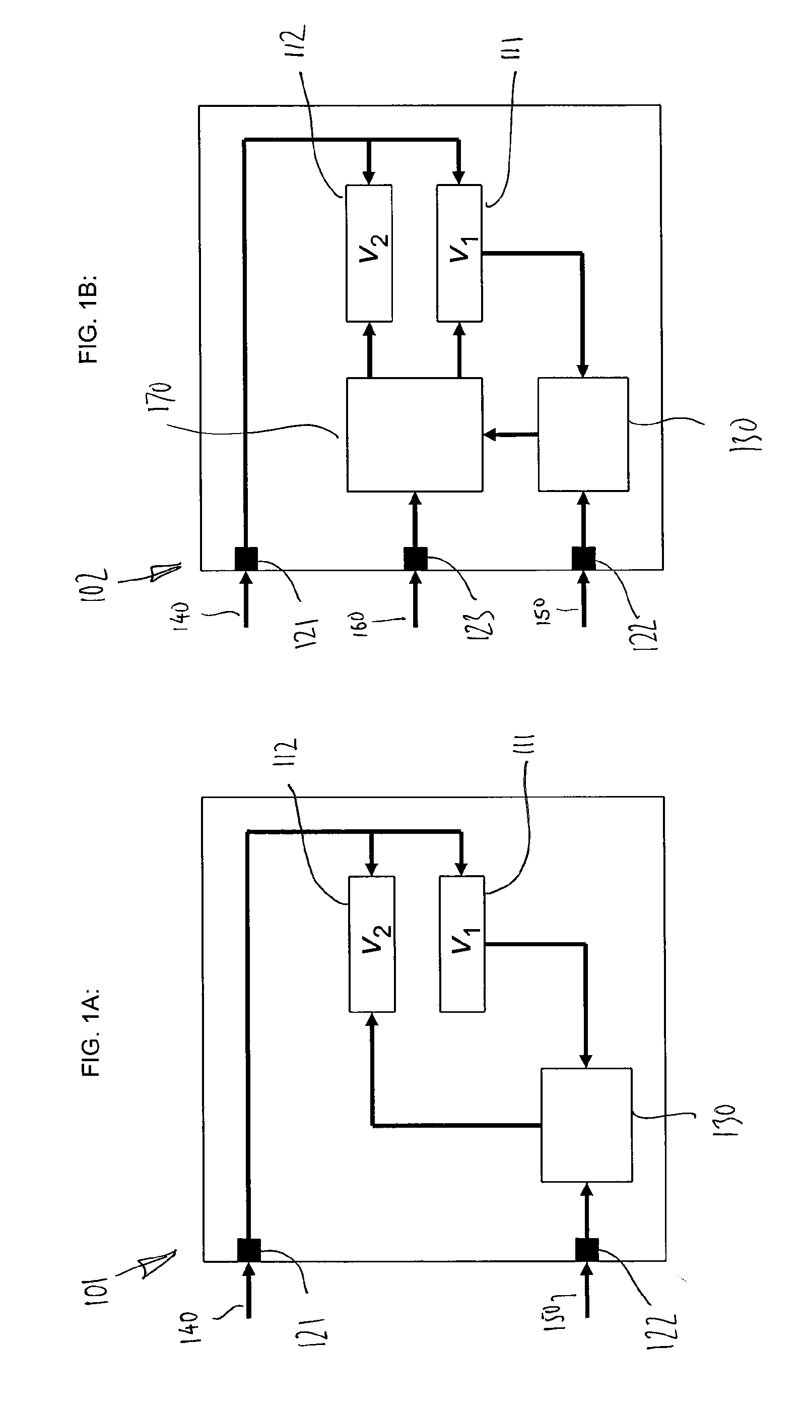
[0019]FIG. 1A shows a schematic view of an integrated device according to a An integrated device 101 may comprise a first port 121 and a second port 122. The integrated device 101 further comprises a first register 111 and a second register 112. Also, the integrated device 101 comprises a logic unit 130. The integrated device 101 may be or comprise, for example, a memory device, a microprocessor, a programmable logic device, a DRAM, a GDRAM, a GDDR-DRAM, a central processing unit (CPU), or a graphics processing unit (GPU).

[0020]The first port 121 receives data 140 to be written into the first register 111 and into the second register 112. In this way, a first register value v1 or a second register value v2 may be stored in the registers 111,112. The second port 122 receives data 150. This data 150 may comprise a signal, such as a high level signal and / or a low level signal, and / or command data, user data, and / or address data. The data 150 may comprise a mirroring signal (MF) in ord...

second embodiment

[0024]FIG. 1B shows a schematic view of an integrated device according to a An integrated device 102 may comprise elements, parts, and / or entities of the integrated device 101 as they have been described in conjunction with FIG. 1A. Hence, reference is made here to the elements, parts and / or entities wearing corresponding reference numbers. According to this embodiment, the integrated device 102 comprises a third input 123 and an addressing unit 170. The addressing unit 170 receives address data 160 from the third input 123. Furthermore, the addressing unit 170 is coupled to the logic unit 130. The addressing unit 170 is further coupled to the first register 111 and the second register 112 and determines which of the connected registers 111, 112 is to be written to, depending on the address data being received from the address port 123. A register value, such as the first register value v1 and the second register value v2, are received from the first port 121 by means of data 140. ...

third embodiment

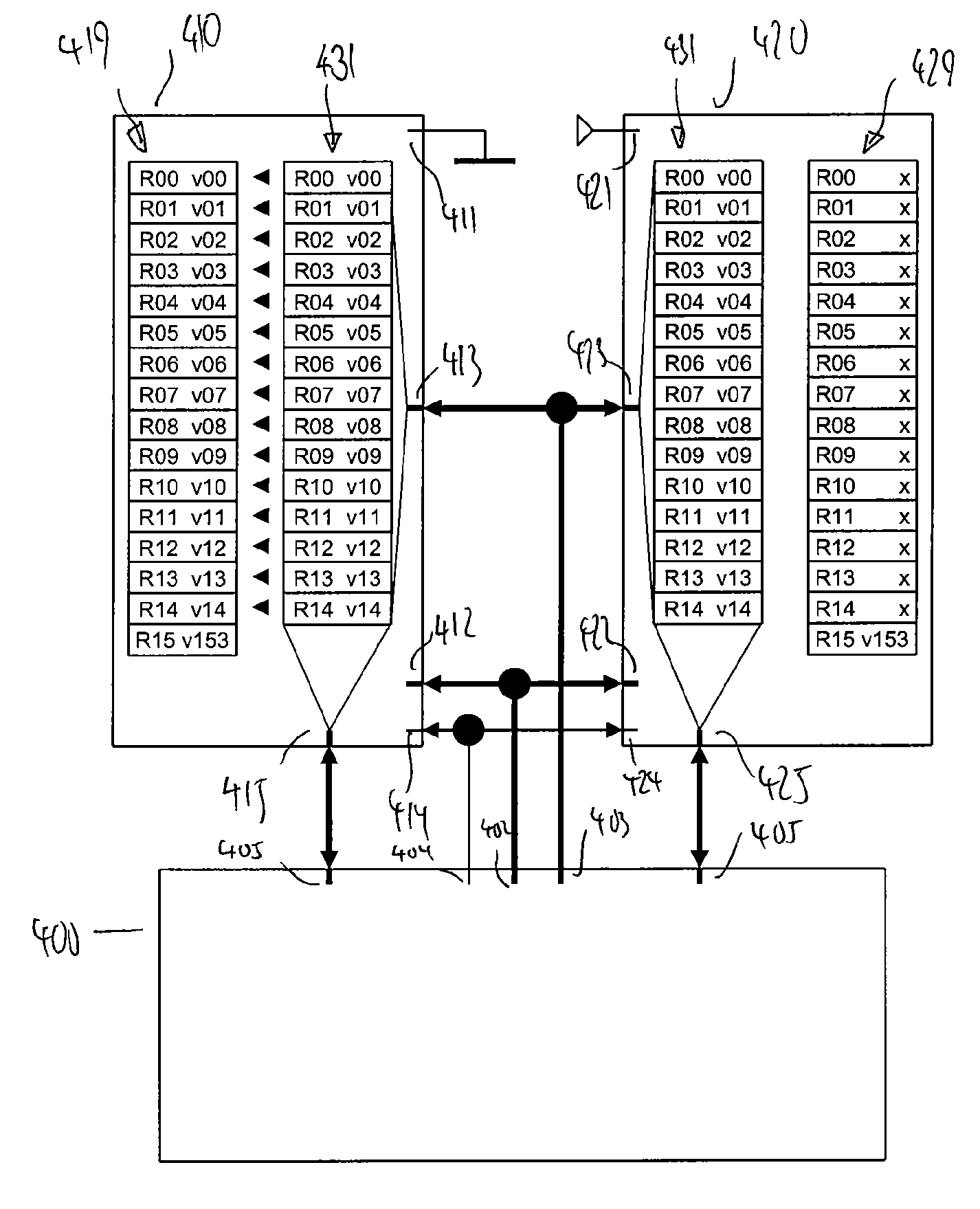
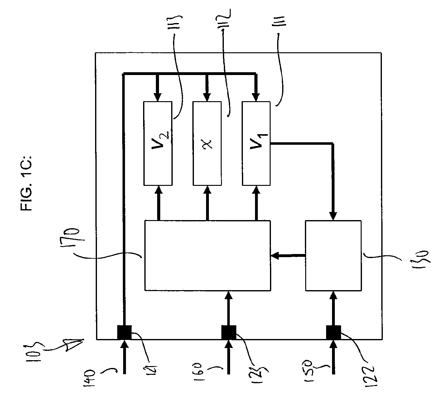
[0026]FIG. 1C shows a schematic view of an integrated device according to a An integrated device 103 may comprise elements, parts, and / or entities of the integrated device 101 and / or the integrated device 102 as they have been described in conjunction with FIGS. 1A and 1B. Hence, reference is made here to the elements, parts and / or entities wearing corresponding reference numbers.

[0027]According to this embodiment the integrated device 103 comprises a third register 113. The third register 113 may store a register value, such as the second register value v2. The addressing unit 170 may re-route a register value v2 into the third register 113, even if the corresponding address data 160, being received from the third input 123, addresses the second register 112. This decision, whether to use a received address or to alter, re-map, or re-address the received address, may be made according to an input from the logic unit 130. Re-routing may be effected by means of increasing or decreas...


PUM


Abstract

A memory device comprises a first port receiving a first register value and a second register value; a second port, receiving a third value; a first register being set to the first register value; a second register having an enabled status and a disabled status, the register being set to the second register value in the enabled status, the second register remaining unchanged in the disabled status; and a logic unit setting the status of the second register dependent on the first register value and the third value.

Description

BACKGROUND OF THE INVENTION[0001]Demands imposed on large scale integrated circuits are constantly increasing. In the case of memory devices, said demands mainly translate into speed and storage capacity. As far as high speed memory devices are concerned, the computer industry has established the so-called DRAM (Dynamic Random Access Memory) as economic means for high speed and high capacity data storage. In somewhat special applications, such as graphic adaptors and graphics cards, the industry has established specialized types, such as GDRAM (Graphics Dynamic Random Access Memory) or the GDDR (Graphics Double Data Rate) memory devices.[0002]Although a DRAM requires a continuous refreshing of the stored information, speed and information density, combined with a relatively low cost, have put the DRAM to a pivotal position in the field of information technology. Almost every modern computer system, ranging, for example, from PDAs over notebook computers and personal computers to hig...

Claims


Application Information

Patent Timeline
IPC IPC(8): G06F3/00
CPCG11C7/1045G11C7/1078G11C7/109G11C11/4096
Inventor HEIN, THOMASMOELLER, UDO
Owner QIMONDA
Why Eureka
Try Eureka