Photomask blank, photomask and method for producing those
a technology of photomask and photomask, which is applied in the field of photomask blank, photomask and method for producing those, can solve the problems of difficult to transfer the shape of the photomask pattern, the shape of the pattern is apt to deteriorate, and the lithography technique for patterning a photomask requires a limited resolution equal or higher, so as to reduce the load on the resist mask, and high precision
- Summary
- Abstract
- Description
- Claims
- Application Information
AI Technical Summary
Benefits of technology
Problems solved by technology
Method used
Image
Examples
embodiment 1
(Basic Configuration of a Photomask Blank)
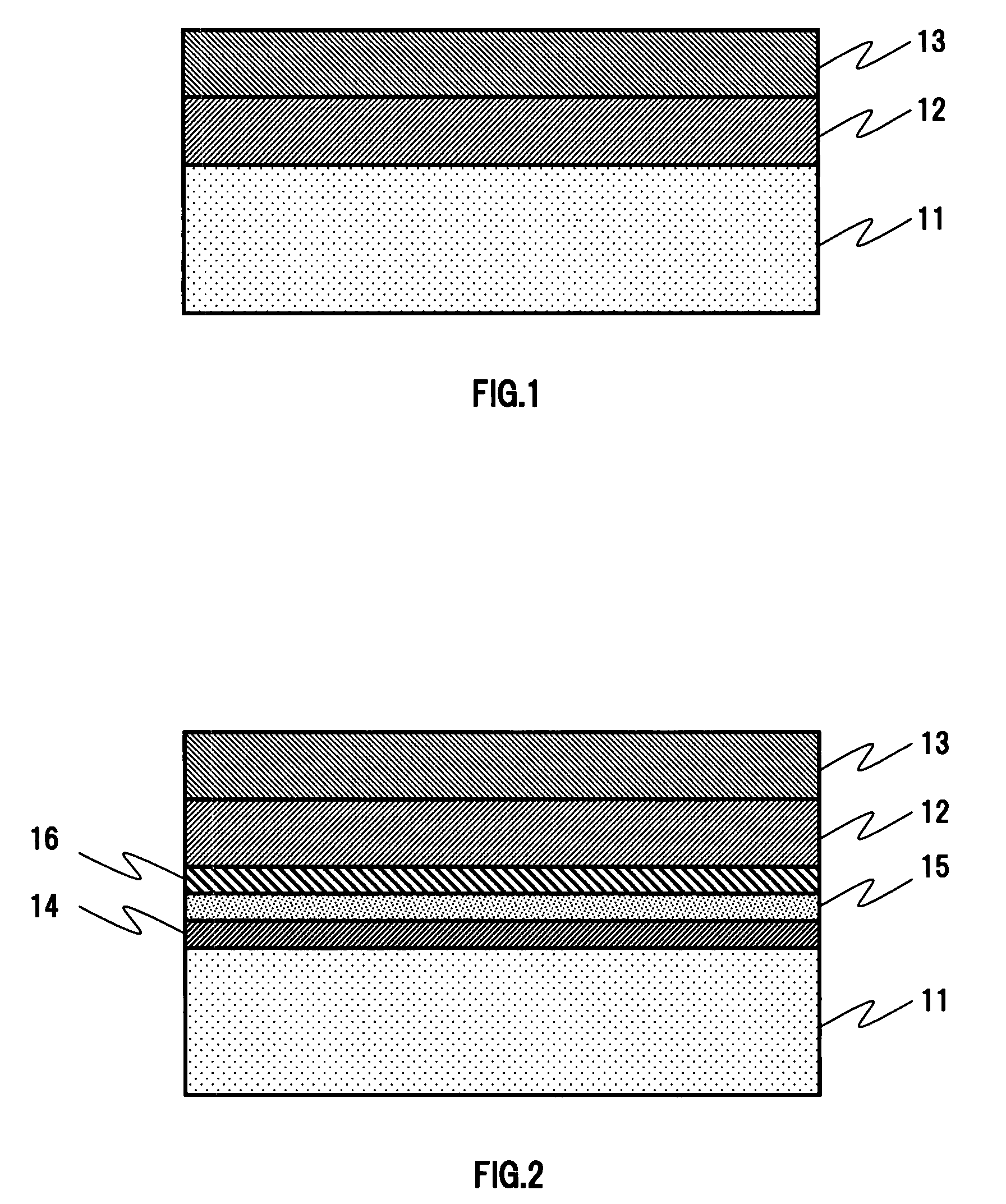
[0041]FIG. 1 is a sectional schematic view for explaining an example of the basic configuration of a photomask blank of the present invention. The photomask blank includes, on one principle surface of a photomask substrate 11, a metal film as a light shielding layer 12. The metal film cannot be substantially etched by chlorine-based dry etching containing oxygen ((Cl+O)-based dry etching) and can be etched by chlorine-based dry etching not containing oxygen (Cl-based dry etching) and fluorine-based dry etching (F-based dry etching). The photo mask blank further includes, on the light shielding layer 12, a metal compound film as an antireflective layer 13. The metal compound film cannot be substantially etched by chlorine-based dry etching not containing oxygen (Cl-based dry etching) and can be etched by at least one of chlorine-based dry etching containing oxygen ((Cl+O)-based dry etching) and fluorine-based dry etching (F-based dry etching)...
embodiment 2
(Phase Shift Mask Blank)
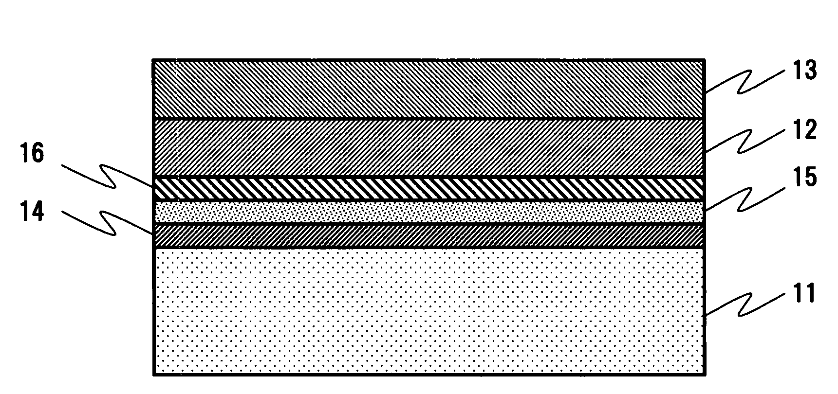
[0062]A mask blank of the present invention may be configured as a phase shift mask blank.
[0063]FIG. 2 is a sectional schematic view for explaining a structural example of a photomask blank of the present invention. The photomask blank is configured as a phase shift mask blank. A transparent or translucent phase shift layer 16 is provided on one principle surface of a photomask substrate 11. A light shielding layer 12 and an antireflective layer 13 (described above) are sequentially stacked on the phase shift layer 16. A variety of known phase shift films can be used for the phase shift layer 16, and the phase shift layer 16 may be a composite film formed by combining these films. Further, the absorber material of the phase shift layer 16 may be replaced with a halftone material to form a halftone phase shift layer.
[0064]Layers denoted as 14 and 15 in FIG. 2 are a buffer layer and an etching stopper layer. These layers are not always necessary but are provide...
embodiment 3
Example 1 of the Processing Process of a Photomask Blank
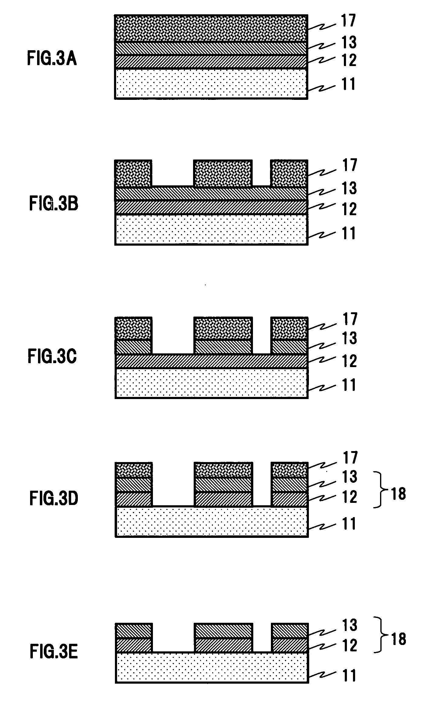
[0070]In the present embodiment, an example of the processing process of a photomask blank will be described. The photomask blank includes an antireflective layer of a chromium compound. In the following explanation, the photomask blank is a so-called binary mask blank (see FIG. 1) in which only a light shielding layer and the antireflective layer are provided on a transparent photomask substrate.
[0071]FIGS. 3A to 3E are process drawings for explaining the processing process of the present embodiment. First, a light shielding layer 12 including a metal film having the composition and thickness described in Embodiment 1 and an antireflective layer 13 made of a chromium compound are sequentially stacked on a transparent photomask substrate 11. A resist film 17 is formed on the antireflective layer 13(FIG. 3A). In order to prevent the occurrence of problems such as the exfoliation and falling of a fine pattern in the subsequent pr...
PUM
| Property | Measurement | Unit |
|---|---|---|
| thickness | aaaaa | aaaaa |
| thickness | aaaaa | aaaaa |
| thickness | aaaaa | aaaaa |
Abstract
Description
Claims
Application Information


