
Photomask Blank, Photomask and Method for Producing Those

Active Publication Date: 2007-11-08
SHIN ETSU CHEM IND CO LTD +1
View PDF4 Cites 26 Cited by
  • Summary
  • Abstract
  • Description
  • Claims
  • Application Information

AI Technical Summary

Benefits of technology

[0027] In the present invention, materials having different etching characteristics (different kinds of material) are selected as the materials of the antireflective layer and the light shielding layer, the configuration of a new photomask blank is used for reducing a load on a resist mask by using the etching selectivity during the formation of a photomask pattern, and the compositions and thicknesses of films making up these layers are properly selected, thereby providing a photomask blank that has a configuration capable of reducing a load on the resist mask and forming a fine photomask pattern with high precision and has physical properties required for a defect inspection, and a photomask fabricated using the photomask blank.

Problems solved by technology

When a pattern simply four times as large as the shape of a written circuit pattern is used as a photomask pattern, it is difficult to transfer the shape of the photomask pattern as it is on a resist film due to the influence of interference or the like of light generated during exposure.
However, in reality, a lithography technique for a process of patterning a photomask requires a limited resolution equal to or higher than that of an optical lithography technique for a process of printing a pattern formed on the photomask onto a semiconductor substrate.
Generally, when the aspect ratio of a resist pattern increases, the shape of the pattern is apt to deteriorate, reducing the accuracy of transferring the pattern to a mask layer with the resist pattern serving as an etching mask.
Moreover, in extreme cases, a part of the resist pattern may fall or come off, so that pattern loss may occur.
Thus when etching the light shielding film with a relatively thin resist film serving as a mask, the resist is damaged and the shape of the resist pattern is changed during the etching, so that it becomes difficult to precisely transfer the original resist pattern onto the light shielding film.
However, it is technically difficult to allow a photoresist, which is an organic film, to have etching resistance (plasma resistance) enabling a high resolution and high patterning accuracy.

Method used


Image

  • Photomask Blank, Photomask and Method for Producing Those
  • Photomask Blank, Photomask and Method for Producing Those
  • Photomask Blank, Photomask and Method for Producing Those

Examples


embodiment 1

(Basic Configuration of a Photomask Blank)

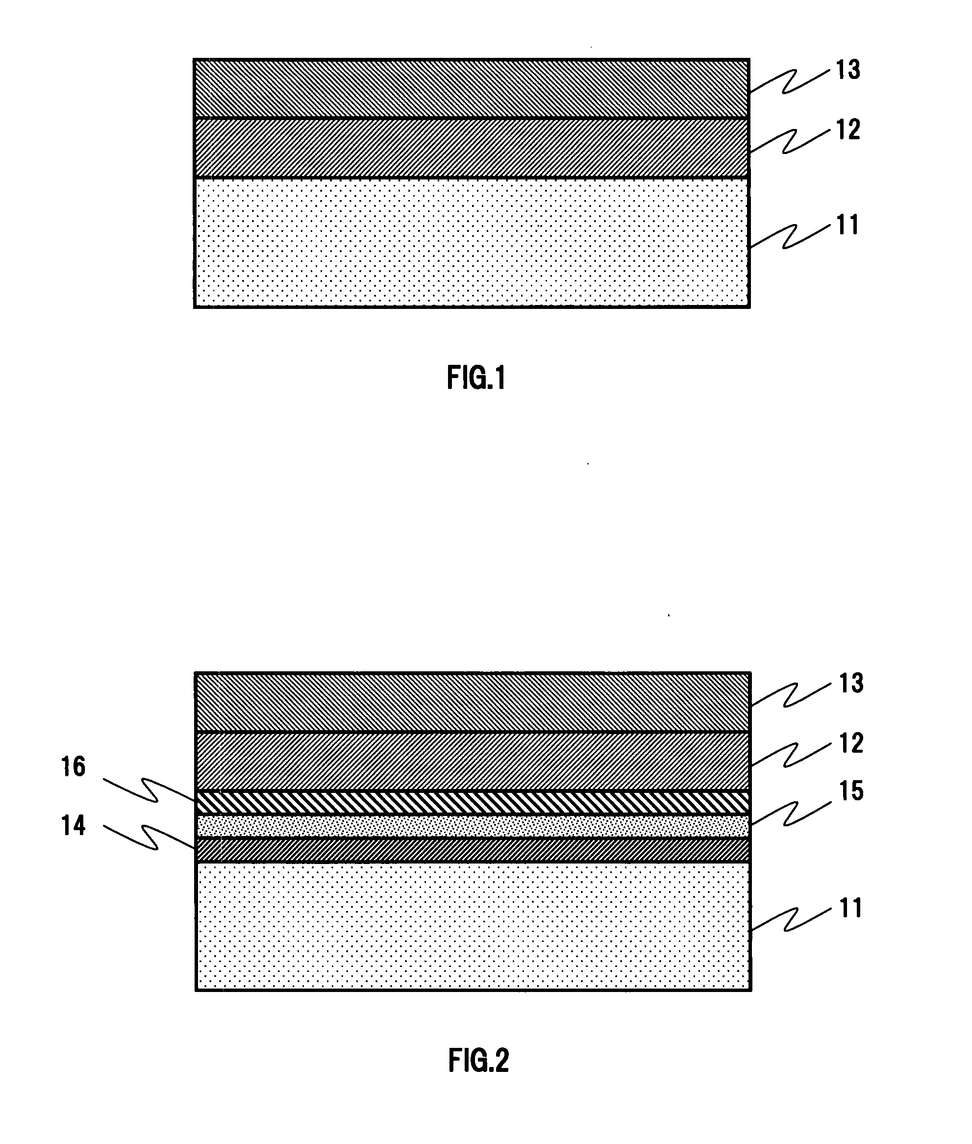
[0047]FIG. 1 is a sectional schematic view for explaining an example of the basic configuration of a photomask blank of the present invention. The photomask blank includes, on one principle surface of a photomask substrate 11, a metal film as a light shielding layer 12. The metal film cannot be substantially etched by chlorine-based dry etching containing oxygen ((Cl+O)-based dry etching) and can be etched by chlorine-based dry etching not containing oxygen (Cl-based dry etching) and fluorine-based dry etching (F-based dry etching). The photo mask blank further includes, on the light shielding layer 12, a metal compound film as an antireflective layer 13. The metal compound film cannot be substantially etched by chlorine-based dry etching not containing oxygen (Cl-based dry etching) and can be etched by at least one of chlorine-based dry etching containing oxygen ((Cl+O)-based dry etching) and fluorine-based dry etching (F-based dry etchin...

embodiment 2

(Phase Shift Mask Blank)

[0067] A mask blank of the present invention may be configured as a phase shift mask blank.

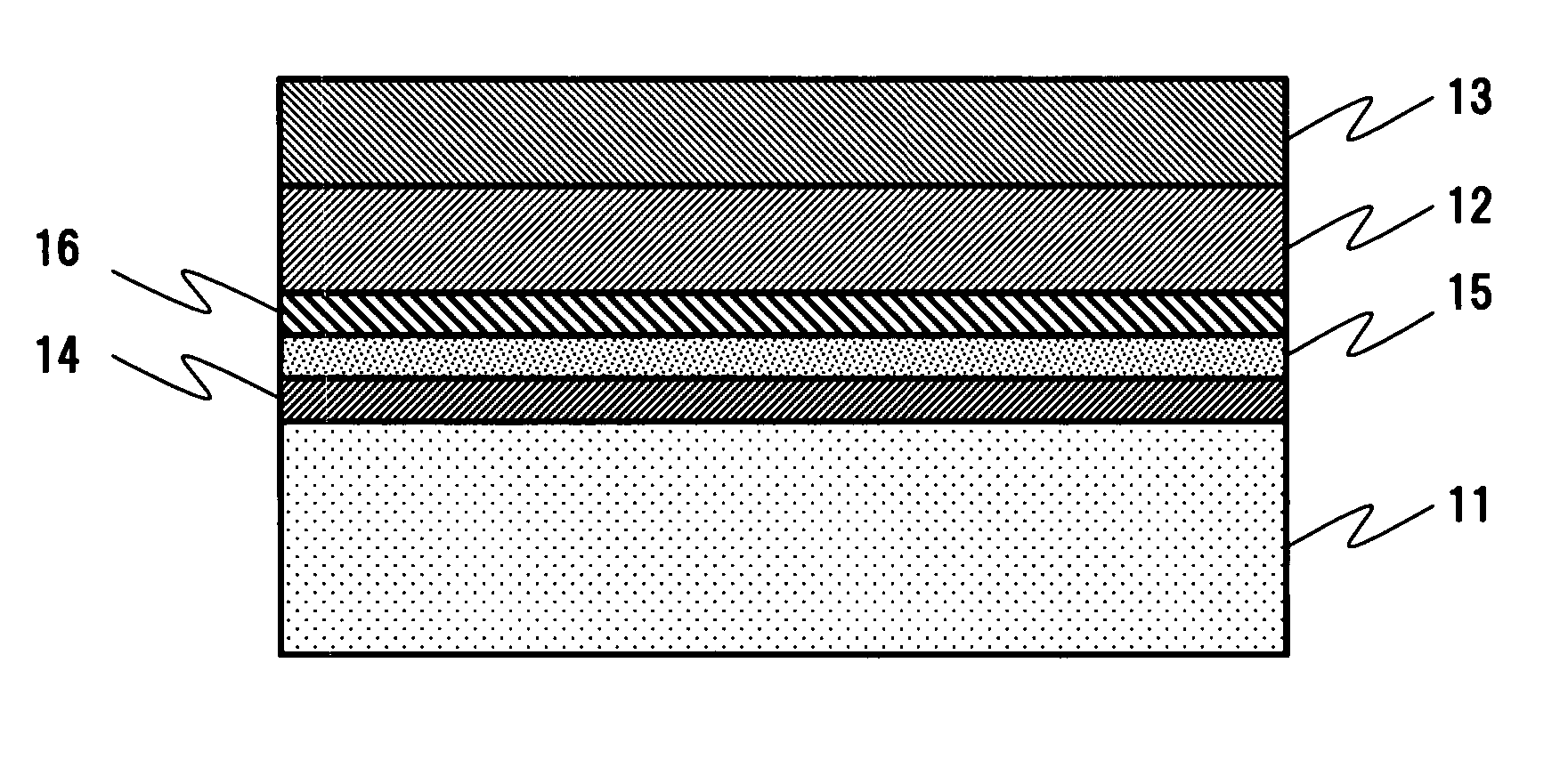
[0068]FIG. 2 is a sectional schematic view for explaining a structural example of a photomask blank of the present invention. The photomask blank is configured as a phase shift mask blank. A transparent or translucent phase shift layer 16 is provided on one principle surface of a photomask substrate 11. A light shielding layer 12 and an antireflective layer 13 (described above) are sequentially stacked on the phase shift layer 16. A variety of known phase shift films can be used for the phase shift layer 16, and the phase shift layer 16 may be a composite film formed by combining these films. Further, the absorber material of the phase shift layer 16 may be replaced with a halftone material to form a halftone phase shift layer.

[0069] Layers denoted as 14 and 15 in FIG. 2 are a buffer layer and an etching stopper layer. These layers are not always necessary but are p...

embodiment 3

(Example 1 of the Processing Process of a Photomask Blank)

[0075] In the present embodiment, an example of the processing process of a photomask blank will be described. The photomask blank includes an antireflective layer of a chromium compound. In the following explanation, the photomask blank is a so-called binary mask blank (see FIG. 1) in which only a light shielding layer and the antireflective layer are provided on a transparent photomask substrate.

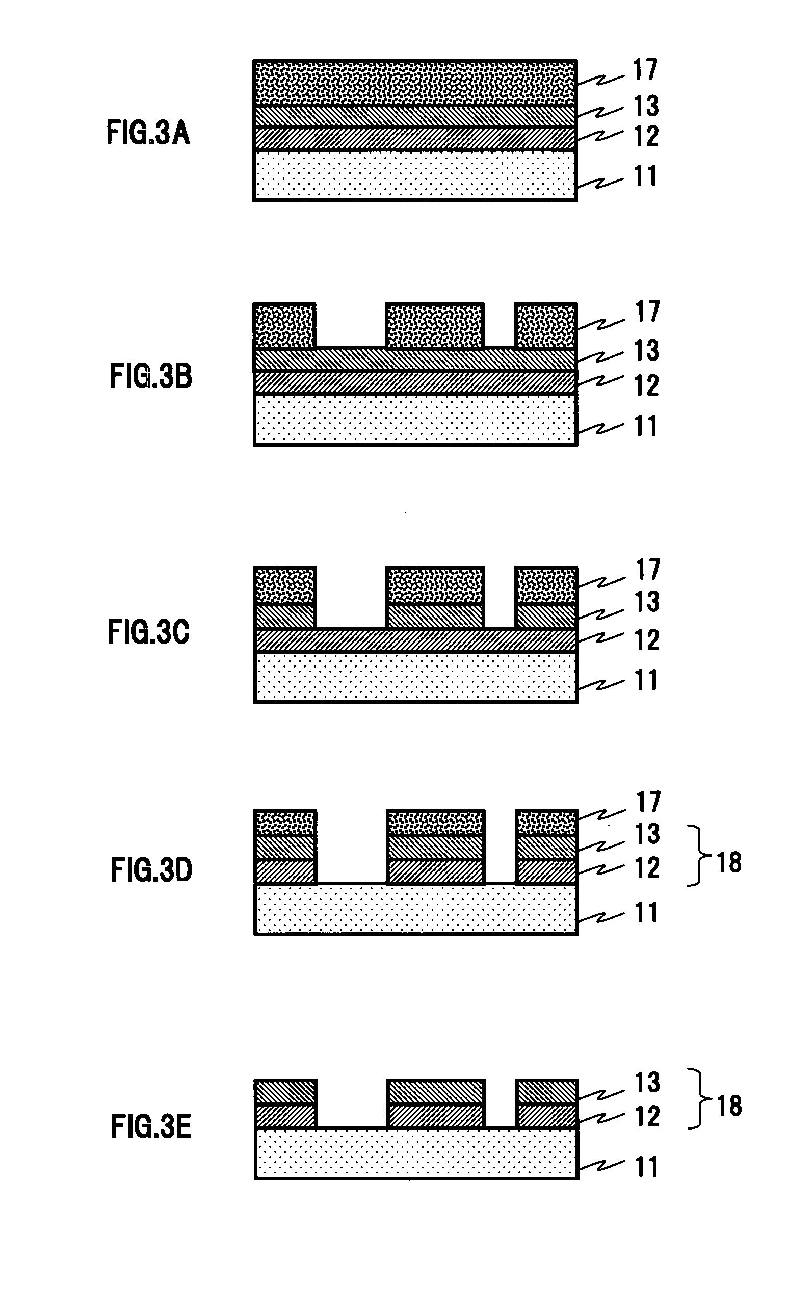
[0076]FIGS. 3A to 3E are process drawings for explaining the processing process of the present embodiment. First, a light shielding layer 12 including a metal film having the composition and thickness described in Embodiment 1 and an antireflective layer 13 made of a chromium compound are sequentially stacked on a transparent photomask substrate 11. A resist film 17 is formed on the antireflective layer 13(FIG. 3A). In order to prevent the occurrence of problems such as the exfoliation and falling of a fine pattern in the subsequ...


PUM

PropertyMeasurementUnit
Thicknessaaaaaaaaaa
Thicknessaaaaaaaaaa
Thicknessaaaaaaaaaa

Abstract

A metal film is provided as a light shielding layer on one principle surface of a photomask substrate. The metal film cannot be substantially etched by chlorine-based dry etching containing oxygen ((Cl+O)-based dry etching) and can be etched by chlorine-based dry etching not containing oxygen (Cl-based dry etching) and fluorine-based dry etching (F-based dry etching). On the light shielding layer, a metal compound film as an antireflective layer. The metal compound film cannot be substantially etched by chlorine-based dry etching not containing oxygen (Cl based) and can be etched by at least one of chlorine-based dry etching containing oxygen ((Cl+O) based) and fluorine-based dry etching (F based).

Description

TECHNICAL FIELD [0001] The present invention relates to techniques for fabricating a photomask blank and a photomask used for fabricating a semiconductor integrated circuit, a CCD (charge-coupled device), a color filter for an LCD (liquid crystal display device), a magnetic head and so on. BACKGROUND ART [0002] Finer circuit patterns have grown in demand in response to finer processing of semiconductor devices in recent years, particularly in response to higher levels of integration of large scale integrated circuits. In order to achieve finer circuit patterns, a technique for making fine lines in a wiring pattern making up a circuit, a technique for making a fine pattern of a contact hole used for wiring between layers making up a cell, and other techniques are necessary. These kinds of patterning have been performed by optical lithography using photomasks, and thus techniques for forming finer photomask patterns with high precision have been demanded. [0003] In order to form a pho...

Claims


Application Information

Patent Timeline
IPC IPC(8): G03F1/08C23F4/00G03F1/14H01L21/027G03F1/48G03F1/50G03F1/54
CPCC23F4/00G03F1/80G03F1/54G03F1/32C03C17/36
Inventor YOSHIKAWA, HIROKIINAZUKI, YUKIOKINASE, YOSHINORIOKAZAKI, SATOSHIHARAGUCHI, TAKASHIIWAKATA, MASAHIDETAKAGI, MIKIOFUKUSHIMA, YUICHISAGA, TADASHI
Owner SHIN ETSU CHEM IND CO LTD
Learn More